


- Semiconductor Materials & Components
- Semiconductor Capital Equipment Market
Semiconductor Capital Equipment Market Size, Share, and Growth Forecast, 2026 - 2033
Semiconductor Capital Equipment Market by Equipment Type (Assembly & Packaging Equipment, Test Equipment, Wafer Fabrication Equipment (WFE)), Application (Foundry/Logic, Memory, Analog, Discrete & Power Devices, Optoelectronics & Sensors, Others), Industry and Regional Analysis for 2026 - 2033
Semiconductor Capital Equipment Market Size and Trends
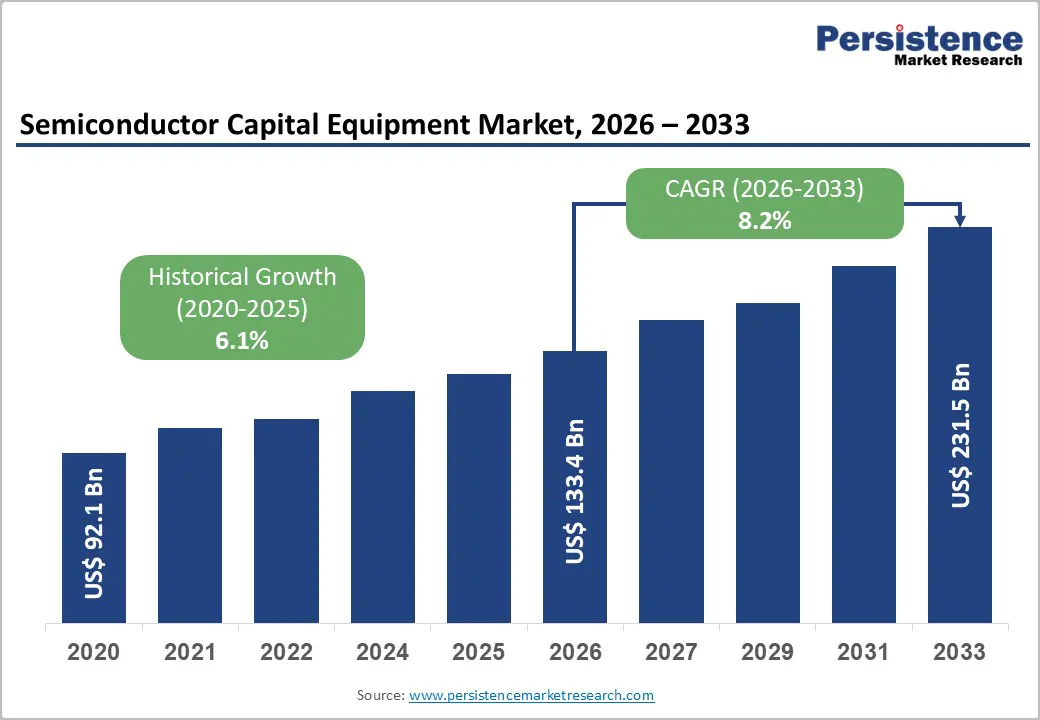
The global semiconductor capital equipment market size is projected to rise from US$133.4 Bn in 2026 to US$231.5 Bn by 2033. It is anticipated to witness a CAGR of 8.2% during the forecast period from 2026 to 2033, driven by accelerating global investments in semiconductor fabrication capacity.
This expansion is largely fuelled by the AI computing boom, 5G infrastructure rollouts, and legislative initiatives such as the U.S. CHIPS and Science Act and the European Chips Act. Advanced process technologies, particularly Extreme Ultraviolet (EUV) and High-NA EUV lithography, are compelling foundries and integrated device manufacturers (IDMs) to procure next-generation fabrication tools. According to SEMI’s Year-End Total Semiconductor Equipment Forecast, global OEM semiconductor equipment sales recorded a 13.7% year-on-year increase, reflecting strong capital expenditure across wafer fabrication facilities worldwide.
Key Industry Highlights:
- Leading Equipment Type: Wafer Fabrication Equipment (WFE) dominates the market with over 84% share in 2026, valued at more than US$ 112 Bn, as it supports critical semiconductor manufacturing processes such as lithography, deposition, etching, and ion implantation required for advanced nodes below 3 nm. Assembly & Packaging Equipment is the fastest-growing, driven by the rise of chiplet architecture, heterogeneous integration, and 2.5D/3D advanced packaging technologies.
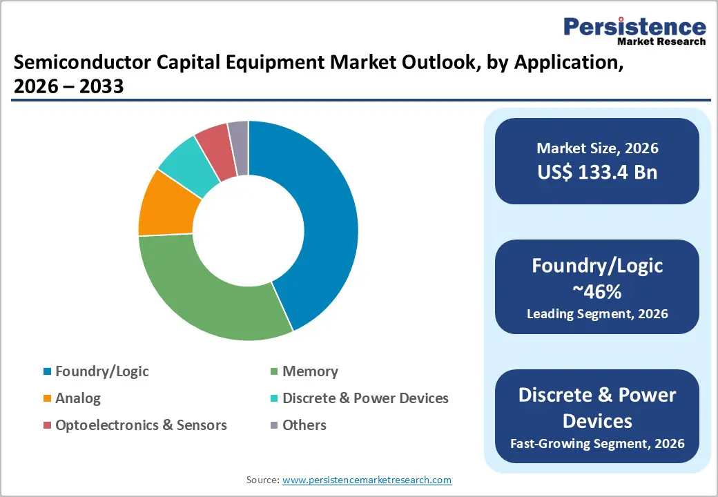
- Leading Application: Foundry/Logic leads with over 46% share in 2026, valued at more than US$ 61.4 Bn, due to increasing demand for advanced processors used in AI, high-performance computing (HPC), and smartphones, alongside the expansion of the fabless semiconductor model. Discrete & Power Devices represent the fastest-growing segment, supported by rising demand for electric vehicles (EVs), renewable energy systems, and high-efficiency power management solutions.
- Leading Industry: Consumer Electronics holds the largest share at over 34% in 2026, valued at more than US$ 45 Bn, driven by massive chip demand for smartphones, laptops, wearables, and smart home devices, as well as rapid product innovation cycles. Automotive is the fastest-growing industry with a CAGR of 11.9%, fueled by increasing semiconductor content in EV powertrains, ADAS systems, battery management, and connected vehicle technologies.
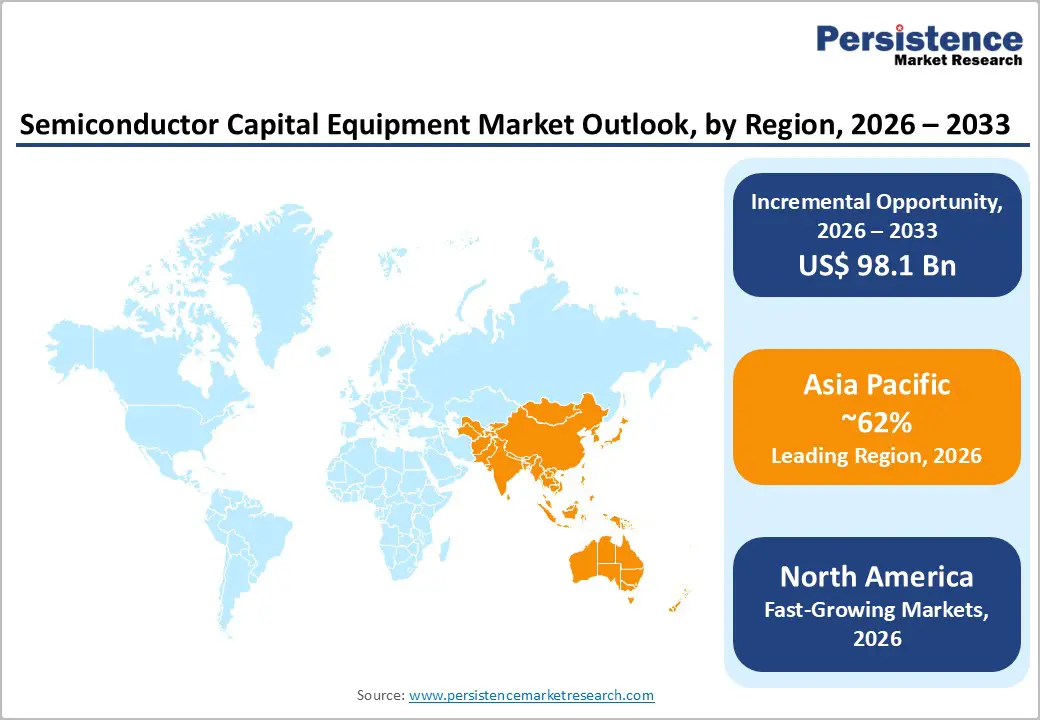
- Leading Region: Asia Pacific leads the global market with over 62% share in 2026, reaching approximately US$ 82.7 Bn, supported by strong fabrication ecosystems in Taiwan, South Korea, Japan, and China, along with continuous investments in advanced nodes and memory production. North America is witnessing significant growth due to new fab investments supported by the U.S. CHIPS and Science Act, while Europe maintains strategic importance through leadership in advanced lithography and semiconductor equipment innovation.
| Key Insights | Details |
|---|---|
| Semiconductor Capital Equipment Market Size (2026E) | US$133.4 Bn |
| Market Value Forecast (2033F) | US$231.5 Bn |
| Projected Growth (CAGR 2026 to 2033) | 8.2% |
| Historical Market Growth (CAGR 2020 to 2025) | 6.1% |
Market Dynamics Analysis
Driver - Surging AI, Cloud, and Advanced Logic Node Investments
The rapid growth of AI workloads, hyperscale cloud computing, and high-performance computing (HPC) is accelerating investments in advanced semiconductor nodes, such as 5 nm, 3 nm, and the upcoming 2 nm. These nodes require highly sophisticated tools, including EUV lithography, advanced deposition, etch, and metrology systems, significantly increasing capital intensity per wafer. Leading chip manufacturers such as TSMC, Intel, and Samsung Electronics are expanding advanced-node capacity to support AI accelerators and data-center chips. Government initiatives like the U.S. CHIPS and Science Act and the European Chips Act are supporting new fab construction, further driving demand for semiconductor capital equipment.
Government-Backed Semiconductor Sovereignty and Capacity Expansion
The push for semiconductor sovereignty and resilient supply chains is prompting record fab construction across the Asia Pacific, North America, and Europe. Countries such as China, Japan, South Korea, India, and Germany are committing multi-billion-dollar incentive packages to attract new fabs and expand existing capacity, spanning logic, memory, analog, and power semiconductors. Asia Pacific already accounts for close to half of global semiconductor capital spending, with some estimates placing regional equipment share at over 45% in 2025, driven by dense foundry ecosystems in Taiwan, South Korea, and China. New fab projects announced in the U.S. and Europe for automotive, industrial, and secure defense chips support long-term demand for both wafer fabrication equipment (WFE) and advanced test solutions.
Restraint - Cyclical Demand, Inventory Corrections, and Macroeconomic Volatility
The semiconductor capital equipment remains exposed to cyclical downturns in end-use electronics, which trigger abrupt cuts in capital expenditure and order pushouts by foundries and IDMs. In 2023, the top five WFE makers saw revenues decline as weak memory spending, soft demand for smartphones and PCs, and macroeconomic uncertainty prompted customers to recalibrate capex plans. The downturn was particularly pronounced in the NAND and DRAM segments, where reduced utilization rates and oversupply further constrained investment in new fabrication capacity. These cycles limit near-term visibility for equipment vendors, elongate sales cycles, and can lead to under-utilized fabs in the short run, thereby dampening new tool purchases until utilization levels recover.
Geopolitical Trade Restrictions and Export Controls
Intensifying geopolitical tensions and export controls targeting advanced semiconductor technologies act as another significant headwind. Restrictions imposed by the U.S. and allied countries on shipping leading-edge lithography and other critical tools to certain regions, particularly China, have constrained the market size available to top vendors and required frequent realignment of shipment plans. For instance, restrictions on advanced DUV immersion and EUV tools to Chinese fabs have forced companies to adjust their product mix and regional sales strategies, increasing compliance costs and planning complexity. Over time, such controls slow technology migration in impacted regions and fragment the global demand landscape, which weighs on the addressable market for leading-edge equipment.
Opportunity - Advanced Packaging, 3D Integration, and Heterogeneous Chiplet Architectures
The proliferation of high-bandwidth memory (HBM), 2.5D/3D packages, and fan-out wafer-level packaging drives demand for high-precision bonding, wafer-level test, and inspection systems that support thousands of interconnects per package at high yields. Industry roadmaps for AI accelerators and data center processors increasingly rely on complex packaging to overcome scaling and bandwidth bottlenecks, shifting more value creation toward assembly and packaging equipment suppliers. Vendors that deliver integrated solutions spanning wafer bumping, hybrid bonding, advanced test, and optical inspection stand to capture outsized growth as advanced packaging becomes a core pillar of the broader semiconductor manufacturing equipment value chain.
Power Electronics, EV, and Wide-Bandgap Semiconductors in Automotive and Industrial
Governments worldwide are mandating stricter efficiency and emissions standards, while EV penetration and grid-scale renewables adoption are rising sharply, boosting demand for discrete and power devices as well as analog and mixed-signal ICs. This opens avenues for equipment designed for wide-bandgap wafers, including high-temperature implantation, epitaxy, and advanced test solutions capable of handling higher voltages and switching speeds. As automotive and industrial OEMs seek secure, local supply for critical power semiconductors, new fabs dedicated to SiC and GaN devices in Europe, North America, and the Asia Pacific will support robust order books for both wafer fabrication equipment (WFE) and back-end assembly tools.
Category-wise Analysis
Equipment Type Insights
Wafer fabrication equipment (WFE) dominates, capturing more than 84% market share in 2026 with a value exceeding US$ 112 Bn, and it is essential for the core manufacturing stage of semiconductor chips. These tools are required for critical wafer-processing steps such as lithography, deposition, etching, ion implantation, and cleaning, which directly define transistor structures and chip performance. As semiconductor nodes shrink to 3 nm and below, fabrication processes become more complex, increasing the need for advanced and highly precise equipment. Massive investments in new semiconductor fabs and rising demand for chips used in AI, 5G, data centers, and automotive electronics further increase the requirement for wafer fabrication tools.
Assembly & packaging equipment is expected to grow rapidly as the complexity of advanced chip packaging increases. As semiconductor manufacturers move toward chiplet architectures, heterogeneous integration, and 2.5D/3D packaging, there is a stronger need for advanced assembly tools and high-precision packaging systems. The rapid growth of AI processors, high-performance computing, and automotive electronics also requires efficient packaging to improve performance, power efficiency, and heat management. Demand for miniaturized consumer electronics and high-density semiconductor devices is driving the need for innovative packaging technologies.
Application Analysis,
Foundry/Logic holds over 46% market share in 2026, with a value exceeding US$ 61.4 Bn, driven by the growing need to manufacture advanced processors for AI, high-performance computing, and smartphones. Foundries must invest heavily in advanced lithography, deposition, and etching equipment to produce smaller technology nodes. The fabless semiconductor business model is increasing reliance on third-party foundries, driving continuous capacity expansion.
Discrete & Power Devices are expected to grow at the highest rate due to the rising need for efficient power management across multiple industries. The rapid expansion of electric vehicles (EVs), renewable energy systems, and fast-charging infrastructure is driving demand for power semiconductors, including IGBTs, MOSFETs, and SiC-based devices. These components are essential for converting and controlling high voltages and currents efficiently. Industrial automation, data centers, and consumer electronics require more reliable power control solutions.
Industry Insights
Consumer Electronics commands the largest market share at over 34% in 2026, with a value exceeding US$ 45 Bn, due to the massive and continuous demand for chips used in smartphones, laptops, tablets, smart TVs, and wearable devices. These products require high-volume semiconductor production, driving strong investment. Rapid product innovation and shorter device replacement cycles also push manufacturers to expand fabrication capacity. Increasing integration of AI processors, sensors, and connectivity chips in consumer devices further raises the need for advanced semiconductor manufacturing equipment.
The automotive industry is expected to grow at a 11.9% CAGR due to the rapid increase in semiconductor content per vehicle. Modern vehicles require advanced chips for electric powertrains, battery management systems, ADAS, infotainment, and vehicle connectivity. The transition toward electric vehicles (EVs) and autonomous driving technologies is significantly increasing demand for power devices, sensors, and microcontrollers. Stricter safety and emission regulations are pushing automakers to integrate more electronic systems.
Regional Insights
North America Semiconductor Capital Equipment Market Trends
North America is expected to reach a significant CAGR supported by strong equipment manufacturers and growing domestic fab investments. The U.S. CHIPS and Science Act allocate over USD 52 billion to expand semiconductor manufacturing, driving new fab projects by companies such as Intel and Samsung Electronics in the U.S. This expansion is boosting demand for wafer fabrication equipment, advanced packaging, and semiconductor test systems, particularly for AI, automotive, and defense chips. The region also hosts major equipment leaders, including Applied Materials, Lam Research, and Teradyne, which drive innovation in etch, deposition, metrology, and test technologies for advanced nodes below 3 nm.
Asia Pacific Semiconductor Capital Equipment Market Trends
Asia Pacific holds over 62% share in 2026, reaching US$ 82.7 Bn value, driven by strong fabrication activity in Taiwan, South Korea, Japan, and China. Leading foundries and memory manufacturers in these countries generate sustained demand for wafer fabrication equipment, assembly & packaging tools, and test systems. Expansion of advanced nodes in Taiwan and capacity upgrades for memory and image sensors in Japan and South Korea further strengthen regional demand. Policy incentives and semiconductor initiatives in India, Vietnam, and Malaysia are encouraging new fabs and supply-chain localization, ensuring Asia Pacific continues to drive global demand for lithography, deposition, etch, inspection, and advanced packaging equipment.
Europe Semiconductor Capital Equipment Market Trends
Europe remains a strategic hub in the semiconductor capital equipment ecosystem due to its leadership in advanced lithography technologies, particularly through ASML Holding in the Netherlands, the global supplier of EUV lithography systems essential for sub-5 nm chip manufacturing. Through the European Chips Act, the European Union aims to mobilize €40+ billion in public and private investments to increase Europe’s semiconductor production share to ~20% by 2030. Countries such as Germany and France are attracting new fabs focused on automotive, industrial, and power semiconductors, supported by strong automotive supply chains. Although large-scale manufacturing remains dominated by Asia, Europe’s leadership in lithography, metrology, and power semiconductor technologies sustains steady demand for high-value semiconductor capital equipment.
Competitive Landscape
The semiconductor capital equipment market is relatively consolidated, dominated by a limited number of highly specialized technology providers. Leading companies differentiate themselves through proprietary technologies, strong research and development capabilities, and long-term partnerships with semiconductor manufacturers. Major players are investing heavily in advanced lithography, process control, and wafer processing technologies. Companies are expanding their service portfolios, including equipment maintenance, software-based process optimization, and predictive analytics solutions.
Key Developments:
- In February 2026, Lam Research Corporation opened a 9,200 sq. ft. office in Boise, Idaho, initially supporting about 150 employees focused on collaborative R&D and manufacturing support for advanced memory chips with Micron Technology, Inc.. The expansion strengthens Lam’s semiconductor equipment innovation and supports growing AI-driven chip manufacturing demand.
- In October 2025, Nikon Corporation announced the availability of its DSP-100 Digital Lithography System, designed for advanced semiconductor packaging. The maskless system uses spatial light modulator technology to deliver 1.0 μm resolution, ±0.3 μm overlay accuracy, and support 600×600 mm substrates. It improves productivity up to 9× compared to wafer processing.
Companies Covered in Semiconductor Capital Equipment Market
- ASML
- Nikon Corporation
- Canon Inc.
- Applied Materials
- Lam Research
- Tokyo Electron
- ASM International
- Hitachi High‑Tech
- Veeco Instruments
- KLA Corporation
- SCREEN Semiconductor Solutions
- Teradyne
- Others
Frequently Asked Questions
The global semiconductor capital equipment market is projected to be valued at US$133.4 Bn in 2026.
Rapid technology node advancements and expanding wafer fabrication capacity worldwide accelerate equipment spending by semiconductor manufacturers are key driver of the market.
The semiconductor capital equipment market is expected to witness a CAGR of 8.2% from 2026 to 2033.
Expansion of advanced semiconductor fabs, AI, and high-performance computing chips is creating strong growth opportunities.
ASML, Nikon Corporation, Canon Inc., Applied Materials, Lam Research, Tokyo Electron, and ASM International are among the leading key players.


