


- Semiconductor Materials & Components
- Compound Semiconductor Material Market
Compound Semiconductor Material Market Size, Trends, Share, and Growth Forecast for 2025 - 2032
Compound Semiconductor Material Market by Application (Consumer Electronics, Energy & Power, Aerospace & Defense, Telecommunication, Automotive), Product Type, and Regional Analysis for 2025 - 2032
Compound Semiconductor Material Market Size and Trends Analysis
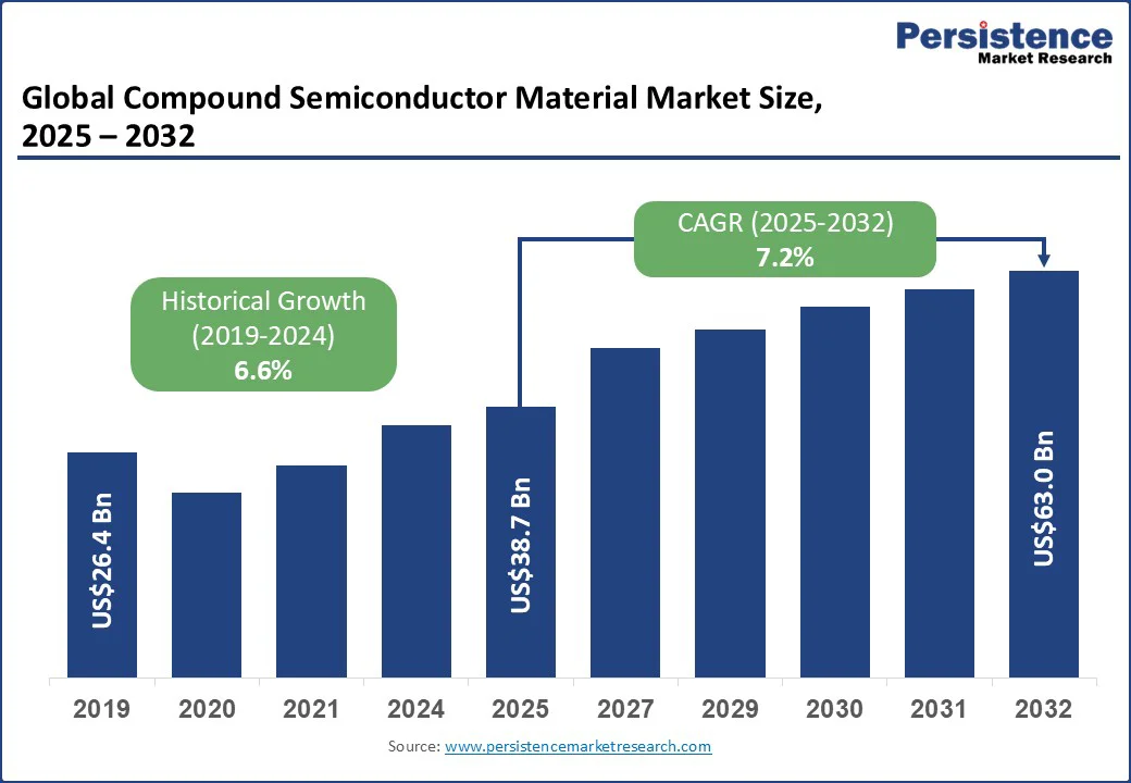
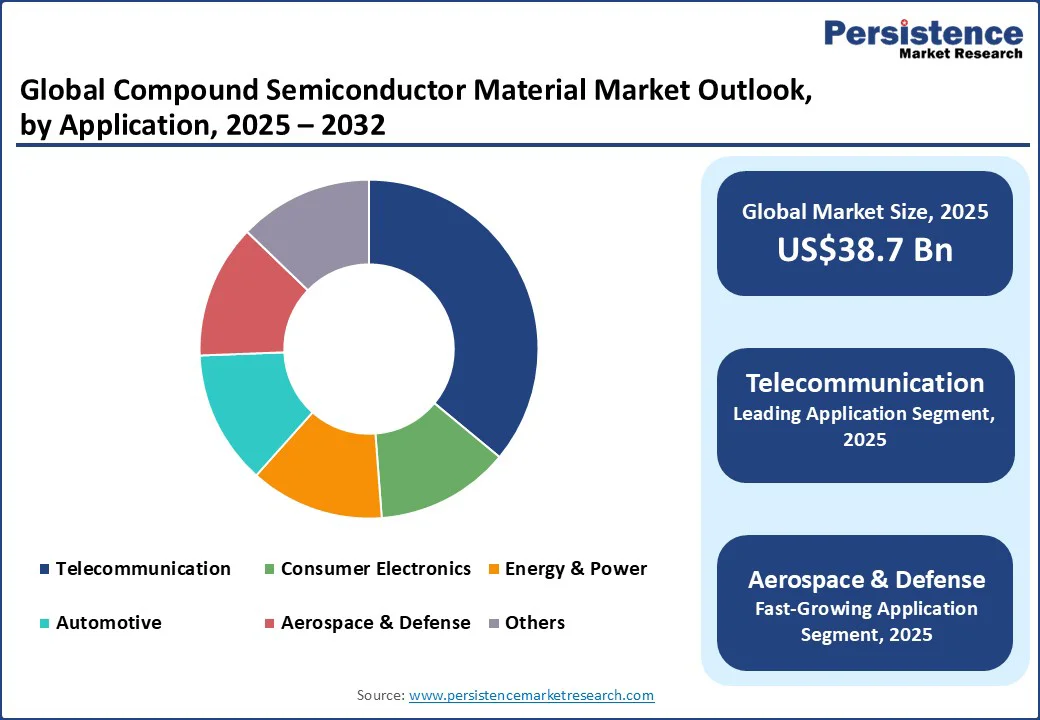
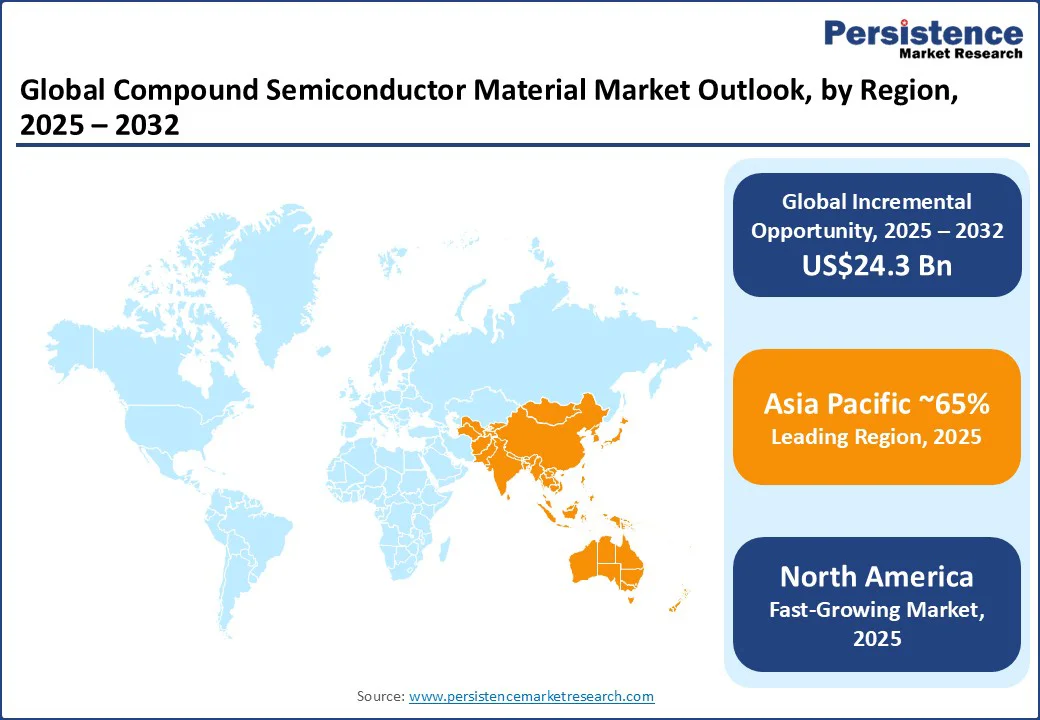
The global compound semiconductor material market size is likely to be valued at US$38.7 Bn in 2025 and is expected to reach US$63.0 Bn by 2032, growing at a CAGR of 7.2% during the forecast period from 2025 to 2032, propelled by rising adoption of wide-bandgap materials such as GaN and SiC in electric vehicles (EVs,) renewable energy, and 5G infrastructure. Unlike conventional silicon, compound semiconductors deliver superior efficiency, higher switching speeds, and better performance in demanding applications.
Key Industry Highlights
- Leading Region: Asia Pacific dominates with around 65% share of the global compound semiconductor materials market, supported by large-scale investments in GaN and SiC foundry projects in China, Taiwan’s SiC R&D centers, and rising adoption in EVs, 5G, and consumer electronics.
- Fastest-Growing Region: North America is advancing rapidly, fueled by the U.S. DoD’s US$280 Mn Microelectronics Commons program and GlobalFoundries’ US$3.1 Bn expansion in GaN and silicon photonics production.
- Dominant Product Type: Gallium Nitride (GaN) holds a leading 45% share in 2024, driven by its efficiency in RF devices, LEDs, and power electronics, with strong adoption in telecom and high-performance electronics.
- Leading Application: Telecommunications is the top application, accounting for a 36% share in 2025, as GaAs, InP, SiGe, and GaN enable 5G base stations, RF modules, and optical transceivers powering global connectivity.
- Key Developments: In August 2025, India approved its first SiC wafer fabrication plant in Bhubaneswar to produce 60,000 wafers annually. In September 2025, Samco Inc. inaugurated an Advanced Technology Development Center in Kyoto with a Class 1000 cleanroom for GaN, SiC, GaAs, and InP research.
| Key Insights | Details |
|---|---|
|
Compound Semiconductor Material Market Size (2025E) |
US$38.7 Bn |
|
Market Value Forecast (2032F) |
US$63.0 Bn |
|
Projected Growth (CAGR 2025 to 2032) |
7.2% |
|
Historical Market Growth (CAGR 2019 to 2024) |
6.6% |
Market Factors – Growth, Barriers, and Opportunity Analysis
Stringent Water Discharge Regulations and Scarcity Concerns
The rollout of 5G infrastructure and electrification trends are powerful growth drivers for the compound semiconductor materials market. Materials such as GaN and GaAs are indispensable for high-frequency and power-efficient RF components in 5G base stations, enabling faster data transmission and lower latency. At the same time, demand from EVs is accelerating, with SiC-based power electronics playing a critical role in improving efficiency in battery management systems and drive inverters.
For example, Wolfspeed has been investing heavily in expanding SiC and GaN wafer production to supply both the automotive and telecom sectors. This dual demand from next-generation communication networks and electric mobility creates a sustained growth environment for compound semiconductor materials, making them central to the transition toward energy efficiency and high-performance electronics.
High Capital and Operating Costs of ZLD Systems
A major restraint in the compound semiconductor materials market is the high production and manufacturing cost, driven by complex processes, expensive raw materials, and advanced equipment needs. For instance, a 6-inch GaN on SiC wafer can cost three to five times more than a comparable silicon wafer, making adoption difficult in cost-sensitive industries.
In addition, manufacturers face supply chain volatility, with many reporting disruptions in raw material procurement in recent years that further pushed up costs and extended lead times. Technical hurdles also limit scalability, as mismatches in lattice structures and thermal properties often result in higher defect rates. Industry estimates suggest that more than one-fifth of GaN devices fail during integration. These financial and technical challenges restrict wider use, especially in consumer electronics and applications where cost efficiency is critical.
Industrial Water Reuse and Circular Economy Initiatives
The rising adoption of photonic technologies in automotive LiDAR and aerospace sensors presents a significant opportunity for compound semiconductors. In the automotive sector, shipments of LiDAR systems based on GaAs and InP materials surpassed half a million units in 2023, reflecting strong integration into advanced driver assistance systems and autonomous vehicle platforms.
In addition, photonic integrated circuits that rely heavily on compound semiconductors are gaining traction in defense and space applications, with unit volumes expanding rapidly across North America and Europe. These materials enable high precision sensing, faster optical communication, and improved performance in extreme environments where silicon falls short. As industries move toward greater reliance on photonics for safety, connectivity, and efficiency, compound semiconductors are positioned to capture long-term opportunities in both automotive and aerospace domains.
Category-wise Analysis
Product Type Insights
Gallium Nitride stands out as the dominant product type in the compound semiconductor materials market, holding a strong share of around 45% in 2025. Known for its high breakdown voltage, excellent thermal stability, and ultra-fast switching, GaN is indispensable in power electronics, RF devices, and high-brightness LEDs. Its ability to deliver miniaturization and superior energy efficiency compared to traditional silicon has secured its lead across multiple industries.
While Silicon Carbide is rising quickly in high-power use cases such as EV inverters and renewable energy, GaN continues to command the largest portion due to its established performance advantage in high-frequency and power-efficient applications.
Application Insights
Telecommunications is the leading application segment in the compound semiconductor materials market, capturing about a 36% share in 2024. The rapid expansion of 5G networks and the surge in mobile data consumption have made materials such as GaAs, InP, SiGe, and GaN essential for enabling high-speed and reliable communication.
Compound semiconductors offer superior electron mobility, faster switching, and higher bandwidth capacity compared to silicon, which makes them vital in RF front-end modules, base stations, and optical transceivers. As global data traffic continues to multiply and next-generation connectivity standards advance, telecommunications remains the backbone application driving large-scale adoption of compound semiconductor materials.
Regional Insights
North America Compound Semiconductor Material Market Trends
North America is a hub for compound semiconductor innovation, driven by robust government and private investments. In 2023, the U.S. Department of Defense (DoD) launched the Microelectronics Commons program, allocating around US$280 Mn to advance semiconductor R&D, including gallium arsenide (GaAs) and gallium nitride (GaN) for defense applications, as part of the CHIPS Act’s US$2 Bn DoD budget. The region leads in GaAs-based photonic systems, producing over 60% of components for aerospace and defense, bolstering communication technologies.
Chip sales in the Americas surged 43.6% year-over-year in May 2025, reaching US$16.6 Bn, fueled by demand for 5G and AI applications. GlobalFoundries is investing US$3.1 Bn, supported by CHIPS Act funds, to expand GaN and silicon photonics production in New York and Vermont. These efforts solidify North America’s leadership in power electronics and next-generation communication infrastructure.
Europe Compound Semiconductor Material Market Trends
Europe is steadily advancing in the compound semiconductor market with a strong focus on sustainability, innovation, and industrial resilience. In 2023, Germany and France together accounted for more than one-third of Europe’s total SiC device output, while France announced plans for more than 14 new fabrication lines focused on GaN on silicon technology. The European Space Agency is actively funding compound semiconductor solutions for satellite communication and space exploration, signaling the region’s commitment to advanced photonics and aerospace technologies.
Automotive giants such as Renault and Volkswagen are increasingly adopting SiC components in their electric vehicle platforms to enhance efficiency and range. These developments reflect Europe’s strategy to lead in sustainable and high-performance technologies, positioning the region as a hub for advanced compound semiconductor adoption in mobility, aerospace, and energy applications.
Asia Pacific Compound Semiconductor Material Market Trends
Asia Pacific dominates the compound semiconductor market with a 65% market share through a combination of large-scale production and rapid technology adoption. In 2023, China committed more than US$3.5 Bn to new GaN and SiC foundry projects, launching over 70 initiatives aimed at strengthening its semiconductor base. Taiwan invested more than US$600 Mn in 18 new research and development centers focused on SiC wafer advancements, reinforcing its role as a key supplier.
Countries such as South Korea and Japan are also expanding efforts in GaAs and InP for 5G infrastructure and optical communication networks. With the region leading global adoption of EVs, high-speed connectivity, and consumer electronics, its dominance in compound semiconductor production is reinforced by both demand and capacity. This synergy makes Asia Pacific the central growth engine for compound semiconductor technologies worldwide.
Competitive Landscape
The global compound semiconductor material market is shaped by a mix of established players and emerging innovators. Wolfspeed is driving advancements in silicon carbide substrates, supported by large-scale wafer production and long-term partnerships with automakers and power electronics manufacturers.
STMicroelectronics is investing heavily in integrated SiC production facilities to strengthen its position in the electric vehicle supply chain. Infineon Technologies continues to expand its portfolio across both SiC and gallium nitride, focusing on wide-bandgap solutions for renewable energy and industrial applications.
Onsemi is pursuing vertical integration by securing upstream wafer assets, ensuring greater control over its SiC value chain. Navitas Semiconductor is pushing GaN technology for fast chargers and data centers, while InnoScience is rapidly scaling GaN-on-silicon manufacturing to meet demand from consumer and industrial applications. Together, these strategies are accelerating innovation and strengthening the global compound semiconductor ecosystem.
Key Industry Developments:
- In August 2025, the Indian government approved the country’s first SiC wafer fabrication plant in Bhubaneswar, led by SiCSem and the U.K.-based Clas-SiC. The facility will produce around 60,000 wafers and 96 million devices annually, targeting EVs, defense, rail, fast chargers, and solar inverters.
- In September 2025, Samco Inc. opened a new Advanced Technology Development Center in Kyoto with a Class 1000 cleanroom and advanced tools for SiC, GaN, GaAs, and InP. The center aims to accelerate next-gen compound semiconductor processing innovation.
Companies Covered in Compound Semiconductor Material Market
- Nichia Corporation
- Wolfspeed, Inc.
- Qorvo
- Sumitomo Electric Industries, Ltd.
- JX Nippon Mining & Metals
- Shin-Etsu Chemical Co., Ltd.
- SHOWA DENKO K.K.
- STMicroelectronics NV
- Galaxy Compound Semiconductors Inc.
- Coherent Inc.
- SiCrystal GmbH
- Infineon Technologies AG
- Wafer Technology Ltd.
- Resonac Holdings Corporation
- FURUKAWA CO., LTD.
Frequently Asked Questions
The compound semiconductor material market is projected to reach US$38.7 Bn in 2025, driven by the strong adoption of wide-bandgap materials such as GaN and SiC in EVs, renewable energy, and 5G infrastructure.
By 2032, the compound semiconductor material market is expected to grow to US$63.0 Bn, registering a CAGR of 7.2% between 2025 and 2032.
Asia Pacific leads the market with around a 65% share, supported by large-scale investments in GaN and SiC foundry projects in China, Taiwan’s SiC R&D centers, and growing demand from EVs, 5G, and consumer electronics.
North America is the fastest-growing region, propelled by the U.S. Department of Defense’s US$280 Mn Microelectronics Commons program and GlobalFoundries’ US$3.1 Bn expansion in GaN and photonics production.


