


- Semiconductor Materials & Components
- Semiconductor Lithography Equipment Market
Semiconductor Lithography Equipment Market Size, Share, and Growth Forecast, 2026 - 2033
Semiconductor Lithography Equipment Market by Lithography Type (Deep Ultraviolet (DUV), Extreme Ultraviolet (EUV), Others), End-user (Pure-play Foundries, Integrated Device Manufacturers (IDMs), Others), and Regional Analysis for 2026 – 2033
Semiconductor Lithography Equipment Market Size and Trends Analysis
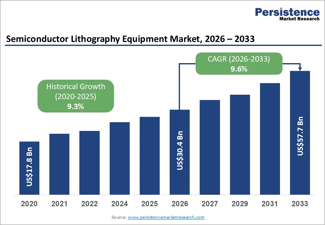
The global semiconductor lithography equipment market size is likely to be valued at US$30.4 billion in 2026, and is expected to reach US$57.7 billion by 2033, growing at a CAGR of 9.6% during the forecast period from 2026 to 2033, driven by the increasing prevalence of advanced node scaling, rising demand for high-resolution patterning in AI chips and 5G devices, and advancements in extreme ultraviolet (EUV) and High-NA EUV technologies. Growing demand for precision lithography equipment, especially in advanced packaging and MEMS devices, is accelerating adoption across end-uses. Advances in DUV and EUV systems are further boosting uptake by offering higher throughput and better yield. Increasing recognition of semiconductor lithography equipment as critical for next-generation chip manufacturing in emerging tech hubs remains a major driver of market growth.
Key Industry Highlights:
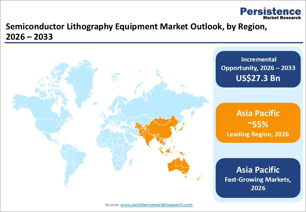
- Leading Region: Asia Pacific, anticipated to lead, accounting for a 55% market share in 2026, driven by dominant foundry capacity, massive chip production, and aggressive expansion in Taiwan, South Korea, and China.
- Fastest-growing Region: Asia Pacific, fueled by government subsidies, rising AI and automotive chip demand, and growing investments in leading-edge fabs.
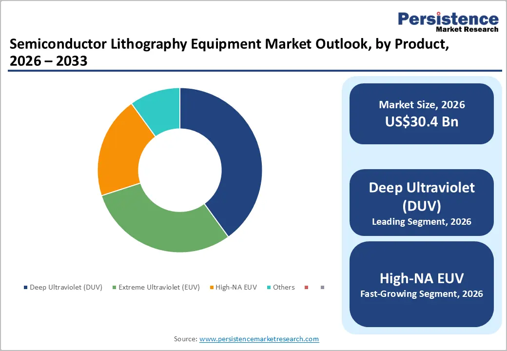
- Dominant Lithography Type: Deep ultraviolet (DUV), to hold approximately 50% of the revenue share, as it remains the workhorse for mature nodes and high-volume production.
- Leading Application: Advanced packaging, to account for over 35% of the market revenue, due to heterogeneous integration and chiplet trends in high-performance computing.
- Leading End-user: Pure-play foundries, to contribute nearly 60% of the market revenue, due to massive capacity expansions by TSMC, Samsung, and Intel.
| Key Insights | Details |
|---|---|
| Semiconductor Lithography Equipment Market Size (2026E) | US$30.4 Bn |
| Market Value Forecast (2033F) | US$57.7 Bn |
| Projected Growth (CAGR 2026 to 2033) | 9.6% |
| Historical Market Growth (CAGR 2020 to 2025) | 9.3% |
Market Factors – Growth, Barriers, and Opportunity Analysis
Rising Demand For Advanced Node Scaling and High-Resolution Patterning
The rising demand for advanced node scaling is quickly becoming a major opportunity for lithography equipment manufacturers, driven by escalating demand for smaller, faster, and more power-efficient chips in AI, 5G, and automotive applications. Traditional DUV lithography faces resolution limits below 7nm, leading to multi-patterning complexity and higher costs. High-resolution technologies, including EUV systems, High-NA EUV tools, advanced DUV scanners, and immersion platforms, address these concerns by offering sub-3nm patterning capabilities. These formats simplify process steps, reduce cycle times, and are particularly effective during 3nm/2nm node transitions where precision is critical.
Semiconductor lithography equipment significantly lowers the risk of yield loss, overlay errors, and cost overruns, which remain major concerns in fab settings. They also support improved throughput and easier integration, especially for EUV and High-NA grades, making them ideal for leading-edge or high-volume fabs. As global semiconductor organizations push for wider Moore’s Law continuation and user-friendly tools, demand continues to expand across advanced packaging, MEMS devices, and LED production.
High Development and Capital Expenditure Costs
High development and capital expenditure costs present a significant barrier for companies advancing next-generation lithography equipment and novel patterning systems. Developing cutting-edge tools such as High-NA EUV scanners, multi-beam e-beam systems, or advanced DUV platforms requires billions in R&D, specialized optics, and precision engineering that are far more expensive than legacy systems. Resolution is an even greater challenge: many next-gen tools, wavelength-shifted optics, and overlay-corrected stages are sensitive to vibration, thermal drift, and source power, requiring rigorous optimization to ensure they remain reliable throughout production. Achieving long-term performance often involves costly field trials, sophisticated metrology testing, and the use of high-grade materials, which significantly increase R&D expenditures.
Meeting stringent customer expectations for throughput, defect density, and batch consistency requires multiple qualification studies under various conditions and across several tool generations. This adds both time and financial burden to development timelines. Scaling up manufacturing requires controlled cleanrooms, specialized lens fabrication, and quality-assurance systems, further driving up overall costs. For smaller players, these challenges can limit technology adoption or delay market entry.
Innovation in EUV and High-NA Delivery Platforms
Advancements in EUV and High-NA lithography equipment delivery platforms are transforming the global semiconductor landscape by addressing two major challenges, resolution limits and cost-per-wafer barriers. EUV platforms are engineered to achieve sub-7nm single-exposure patterning, reducing reliance on multi-patterning and enabling simpler process flows. Innovations, such as high-power plasma sources, pellicle-free masks, anamorphic optics, and high-NA projection systems, significantly improve resolution and throughput, lowering overall fab costs for foundries and IDMs.
Progress in High-NA platforms, including 0.55NA optics, advanced stage synchronization, and AI-driven corrections, supports more aggressive scaling by stimulating sub-2nm capabilities, the industry’s first line of defense against physical limits. These formats eliminate double patterning, enhance overlay, and allow higher productivity without additional steps, making them highly suitable for mass production programs. New technologies such as hyper-NA optics, multi-beam inspection, and VLP-based alignment further enhance yield and cost response.
Category-wise Analysis
Lithography Type Insights
Deep ultraviolet (DUV) is anticipated to dominate the market, accounting for approximately 50% of the market share in 2026. Its dominance is driven by mature node reliability, high throughput, and cost-effectiveness, making it preferred for 7nm and above. DUV systems provide immersion capability, ensure yield, and contribute to volume production, making them suitable for large-scale fab campaigns. ASML Holding N.V., the world’s leading lithography equipment supplier, continues to see broad adoption of its DUV lithography systems, especially ArF immersion DUV scanners in high-volume semiconductor fabs focused on 7 nm and above process nodes. These DUV tools are preferred for mature and mid-node production as they offer high throughput, reliable performance, and relatively lower cost per wafer compared with more expensive EUV systems, which are primarily reserved for the most advanced patterning layers.
High-NA EUV represents the fastest-growing segment, due to its resolution leadership and expanding use in sub-2nm nodes. Its advanced optics profile makes it ideal for targeted scaling, reducing multi-patterning. Continuous innovations in source power are further strengthening their performance, driving rapid adoption across North America and Asia Pacific, where demand for next-generation lithography is accelerating. SK hynix Inc. has assembled and deployed one of the industry’s first commercial High-NA EUV lithography systems, ASML’s Twinscan EXE:5200B, with 0.55 numerical aperture optics at its M16 fab in Icheon, South Korea, targeting next-generation memory and advanced semiconductor production.
Application Insights
Advanced packaging leads the market, holding approximately 35% of the share in 2026, driven by heterogeneous integration needs, large chiplet programs, and strong global demand for high-density interconnects. Their dominance continues as foundries expand 2.5D/3D packaging. Rising adoption of MEMS devices and expanded LED campaigns highlight the growing focus on diverse applications. Taiwan Semiconductor Manufacturing Company (TSMC) has established a commanding position in the advanced packaging sector through its CoWoS® (Chip-on-Wafer-on-Substrate) and SoIC (System on Integrated Chips) technologies, both of which enable 2.5D and 3D heterogeneous integration for high-performance computing, AI accelerators, and memory applications. These platforms allow multiple dies and high-bandwidth memory stacks to be integrated with very fine interconnect density, reducing latency and power consumption compared to traditional packaging approaches.
The MEMS segment is experiencing the fastest growth, driven by strong demand for sensors and the increasing integration of micro-actuators in automotive and IoT applications. The adoption of MEMS devices is being accelerated by the industry’s shift toward miniaturized, high-precision platforms and improved manufacturing yields. Innovations in high-resolution DUV lithography, along with ongoing EUV MEMS production trials, are further supporting market expansion. Bosch Sensortec, a subsidiary of Robert Bosch GmbH, has been broadening its MEMS sensor portfolio, which includes high-precision accelerometers, pressure sensors, and motion modules widely used in automotive safety systems such as ADAS and TPMS, as well as in IoT-connected devices such as wearables and smart home products. The company recently launched the SMP290 MEMS sensor featuring integrated Bluetooth Low Energy, enhancing connectivity for tire pressure monitoring systems (TPMS). This product exemplifies the growing adoption of multifunctional MEMS solutions that combine sensing and communication capabilities for both automotive and IoT applications.
End-user Insights
Pure-play foundries are expected to dominate the market, with approximately 60% share in 2026, due to the high volume of leading-edge wafer production and strong global emphasis on process scaling. Regular lithography schedules, node requirements, and widespread access to EUV tools drive consistent demand. Rising focus on IDMs and OSAT further strengthens pure-play leadership. For example, foundry operators such as TSMC administer EUV lithography for routine 3nm lines, ensuring high coverage in wafers while supporting preventive yield initiatives.
Integrated Device Manufacturers (IDMs) are likely to be the fastest-growing field, fueled by the rising need for custom chips, vulnerability to supply chain risks, and expanding adoption of in-house advanced nodes. Improved control, tailored processes, and stronger innovation for proprietary designs support rapid uptake. The growing use of OSAT, advanced packaging, and others among vertical integration sectors further accelerates market growth. For example, IDM programs such as Intel provide targeted EUV lithography for internal fabs, protecting innovation and reducing the risks of external dependency in high-performance computing.
Regional Insights
North America Semiconductor Lithography Equipment Market Trends
North America is supported by the region’s advanced chip design ecosystem, strong research and development capabilities, and high public awareness of technology leadership benefits. Fab systems in the U.S. and Canada provide extensive support for lithography programs, ensuring wide accessibility of equipment across foundries, IDMs, and OSAT populations. Increasing demand for EUV, convenient, and easy-to-integrate tools is further accelerating adoption, as these formats improve yield and reduce barriers associated with legacy DUV.
Innovation in lithography equipment technology, including stable High-NA optics, improved overlay delivery, and targeted AI correction, is attracting significant investment from both public and private sectors. Government initiatives and CHIPS Act campaigns continue to promote use against node scaling, supply chain security, and emerging AI threats, creating sustained market demand. The growing focus on advanced packaging and MEMS uses, particularly for foundries and others, is expanding the target applications for lithography equipment.
Europe Semiconductor Lithography Equipment Market Trends
Europe is stimulated by increasing awareness of technology sovereignty, strong fab systems, and government-led semiconductor programs. Countries such as Germany, France, and the Netherlands have well-established manufacturing frameworks that support routine lithography and encourage the adoption of innovative equipment delivery methods, including EUV tools. These advanced formulations are particularly appealing for foundry populations, innovation-focused IDMs, and OSAT users, improving yield and coverage rates.
Technological advancements in lithography equipment development, such as enhanced High-NA projection, application-targeted delivery, and improved throughput grades, are further boosting the market potential. European authorities are increasingly supporting research and trials for equipment against both routine and specialized needs, strengthening market confidence. The growing emphasis on sustainable, high-efficiency options is aligned with the region’s focus on preventive scaling and reducing energy consumption. Public awareness campaigns and funding drives are expanding reach in both urban and rural areas, while suppliers are investing in optics and novel sources to increase efficacy.
Asia Pacific Semiconductor Lithography Equipment Market Trends
Asia Pacific is projected to dominate and is likely to be the fastest-growing, holding approximately 55% of the revenue share, fueled by rising fab investments, increasing government initiatives, and expanding application programs across the region. Countries such as Taiwan, South Korea, China, and Japan are actively promoting lithography campaigns to address AI chip growth and emerging advanced node needs. Lithography equipment is particularly attractive in these regions due to its high-precision administration, ease of scaling, and suitability for large-scale fab drives in both urban and rural populations.
Technological advancements are supporting the development of stable, effective, and easy-to-deploy lithography equipment, which can withstand challenging production conditions and minimize defect dependence. These innovations are critical for reaching new fabs and improving overall yield coverage. Growing demand for advanced packaging, MEMS devices, and LED applications is contributing to market expansion. Public-private partnerships, increased semiconductor expenditure, and rising investments in EUV research and manufacturing capacity are further accelerating growth. The convenience of equipment delivery, combined with improved resolution and reduced risk of yield loss, positions lithography equipment as a preferred choice.
Competitive Landscape
The global semiconductor lithography equipment market features competition between dominant EUV leaders and established DUV providers. In North America and Europe, ASML leads through strong R&D, distribution networks, and foundry ties, bolstered by High-NA innovation and process programs. In Asia Pacific, Nikon Corporation and Canon Inc. advance with localized DUV solutions, enhancing accessibility. High-resolution delivery boosts yield, cuts overlay risks, and enables mass node transitions across regions. Strategic partnerships, collaborations, and acquisitions merge expertise, expand tool lines, and speed commercialization. Next-gen formulations solve resolution issues, aiding penetration in advanced nodes.
Key Industry Developments
- In December 2025, Chinese scientists reportedly developed a prototype machine in a high-security Shenzhen laboratory capable of manufacturing advanced semiconductor chips that are critical for powering artificial intelligence, smartphones, and key military technologies, according to Reuters.
- In September 2025, SCREEN Semiconductor Solutions Co., Ltd. and IBM announced a partnership to develop cleaning processes for next-generation EUV lithography. This collaboration expands on their earlier joint efforts, which produced innovative cleaning techniques that supported the development of current-generation nanosheet device technology.
Companies Covered in Semiconductor Lithography Equipment Market
- ASML
- Nikon Corporation
- Canon Inc.
- Carl Zeiss AG
- Veeco Instruments Inc.
- Ushio Inc.
- MKS Instruments (Newport)
- Mapper Lithography B.V.
Frequently Asked Questions
The global semiconductor lithography equipment market is projected to reach US$30.4 billion in 2026.
The rising prevalence of advanced node scaling and demand for high-resolution patterning are key drivers.
The semiconductor lithography equipment market is poised to witness a CAGR of 9.6% from 2026 to 2033.
Advancements in EUV and High-NA delivery platforms are the key opportunities.
ASML, Nikon Corporation, Canon Inc., Carl Zeiss AG, and Veeco Instruments Inc. are the key players.


