


- Semiconductor Materials & Components
- Semiconductor Assembly and Testing Services Market
Semiconductor Assembly and Testing Services Market Size, Share, and Growth Forecast, 2025 - 2032
Semiconductor Assembly and Testing Services Market By Service Type (Assembly Services and Testing Services), Packaging Type (Dual In-line Package (DIP), Quad Flat Package (QFP), Flip-Chip Package, Others), Application, End-user, and Regional Analysis for 2025 - 2032
Semiconductor Assembly and Testing Services Market Size and Trends Analysis
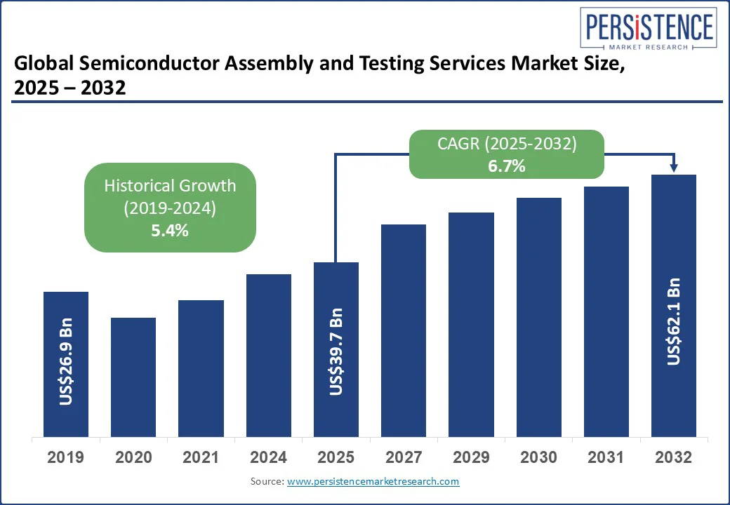
The global semiconductor assembly and testing services market size is likely to be valued at US$39.7 Bn in 2025 and is expected to reach US$62.1 Bn by 2032, growing at a CAGR of 6.7% during the forecast period from 2025 to 2032. Semiconductor assembly and testing services refer to outsourced services that handle the back-end processes in semiconductor manufacturing. These services are crucial for ensuring the functionality, reliability, and performance of semiconductor devices. The increasing chip complexity and miniaturization, along with the adoption of 3D and fan-out wafer-level packaging, have led companies to rely on specialized providers to ensure precision, reliability, and cost control.
Key Industry Highlights
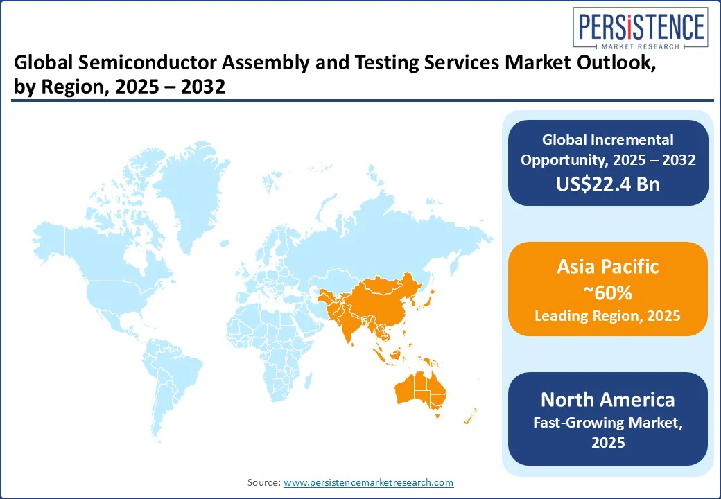
- Leading Region: Asia Pacific dominates the semiconductor assembly and testing services market, accounting for over 60% of global SATS operations, due to its strong manufacturing base, skilled workforce, and the presence of major semiconductor hubs including Taiwan, South Korea, and China.
- Fast- growing Region: North America is the fastest-growing region, driven by rising demand for advanced electronics fueled by innovations in AI, 5G, and autonomous technologies. This has increased the need for high-precision semiconductor assembly and testing services to support domestic manufacturing and ensure supply chain security.
- Dominant Services: Assembly services dominate with over 55% share in 2025, driven by the increasing complexity of semiconductor designs, requiring advanced packaging solutions to ensure performance, miniaturization, and heat management.
- Leading Application: The automotive segment is the fastest-growing, spurred by EV sales exceeding 17 million units in 2024, requiring advanced packaging and rigorous chip testing for ADAS and connected vehicle systems.
- Industry Trend: Fabless semiconductor companies are driving outsourcing growth by relying on third-party providers for advanced packaging and testing. This enables faster time-to-market and reduces capital investment.
- Miniaturization: Heterogeneous integration and miniaturization are shaping the industry, with chiplet-based designs, 2.5D/3D packaging, and FOWLP increasing the need for more advanced testing and assembly services.
|
Global Market Attribute |
Key Insights |
|
Semiconductor Assembly and Testing Services Size (2025E) |
US$39.7 Bn |
|
Market Value Forecast (2032F) |
US$62.1 Bn |
|
Projected Growth (CAGR 2025 to 2032) |
6.7% |
|
Historical Market Growth (CAGR 2019 to 2024) |
5.4% |
Market Dynamics
Driver - Surge in Smart and Connected Devices Drives Demand for Advanced and Rigorous Testing
Consumers and industries are increasingly demanding devices with advanced capabilities such as edge AI, 5G, autonomous vehicles, and smart home automation. To support these applications, chips must undergo multiple rounds of testing, including functional, reliability, and system?level to ensure fault?free operation. For instance, according to Advantest, a leading test equipment supplier, an advanced chip today undergoes testing 10 to 20 times during production, compared to only a few times a few years ago.
In response to this growing complexity, major assembly and testing providers are expanding their operations. Taiwan’s ASE expects its revenue from advanced packaging and testing to rise from about US$600 Mn in 2024 to around US$1.6 Bn in 2025, driven largely by demand for AI-focused chips. Besi, an equipment manufacturer, has also reported a significant increase in hybrid bonding orders since late 2023, with major clients such as TSMC, Intel, and Samsung investing in tools to support AI chip integration and other advanced device requirements.
Restraint - Geopolitical Tensions and Trade Barriers
Rising geopolitical tensions and stricter trade barriers are increasingly constraining the market by interrupting the steady supply of raw materials, equipment, and components essential for production. Governments are imposing tariffs, export controls, and national security measures that raise costs and restrict access to advanced technologies across borders. These policies disrupt established supply chains, making it harder for providers to maintain smooth operations and competitive pricing.
For instance, the U.S. Section?232 investigations launched in April 2025 target semiconductor imports with proposed tariffs starting at 25% and potentially increasing further. Such measures directly impact semiconductor equipment and assembly/testing services originating from key hubs including Taiwan, South Korea, Malaysia, and China. The resulting cost hikes squeeze margins for SATS providers and force them to reconfigure manufacturing and sourcing strategies, leading to delays and higher overall operational expenses.
Opportunity - Heterogeneous Integration Creates Novel Opportunities
Heterogeneous integration is changing how semiconductors are built by combining multiple smaller chips, called chiplets, into a single package. This approach helps create devices that are faster, more power?efficient, and smaller, which is important for new technologies such as AI, 5G, autonomous vehicles, and IoT. This shift also makes chip design more complicated, which means the testing process has to be more advanced to ensure everything works correctly. To meet this need, companies that make automated test equipment (ATE) are developing more capable tools to handle the wide range of functions and connections in these new chip designs, thus accelerating demand for test services.
For instance, according to SEMI, as of March 2024, over 30% of global SATS facilities had adopted advanced packaging techniques such as flip chip, fan?out wafer?level packaging (FOWLP), through?silicon via (TSV), and 2.5D/3D integration. These capabilities reflect a rapid expansion into heterogeneous integration workflows, positioning SATS providers to capture growing opportunities. As chiplet?based designs gain traction, SATS companies equipped to assemble and rigorously test these complex packages stand to benefit from new revenue streams and long?term relevance in the evolving semiconductor landscape.
Semiconductor Assembly and Testing Services Market Key Trend
Miniaturization and Advanced Packaging
The growing demand for smaller, more efficient devices across consumer electronics, automotive, and telecommunications sectors is driving the shift toward miniaturization and advanced packaging in semiconductors. Techniques such as Fan-Out Wafer-Level Packaging (FOWLP), 3D stacking, and Chip-on-Wafer-on-Substrate (CoWoS) enable the integration of multiple functions into compact packages, while also improving performance and power efficiency. These technologies are becoming essential for applications such as 5G, AI, and IoT, where devices must deliver more capabilities in a limited space.
For instance, a recent study by Bhoumik, Bailey, and Chakrabarty illustrates how fan?out wafer-level packaging (FOWLP), while key to achieving higher interconnect density for miniaturized devices, brings complex manufacturing issues such as warpage, die shift, and bonding defects. To address these issues, they proposed a built-in self-test (BIST) framework to detect and diagnose faults in chiplet interconnects, demonstrating how advanced testing solutions are evolving alongside packaging innovations to ensure reliability in increasingly compact semiconductor designs.
Category-wise Analysis
Service Type Insights - Assembly Services Dominate Due to Rising Complexity and Localization Push
Based on service type, the market is segmented into assembly services and testing services. Among these, assembly services are expected to hold over 55% of the market share in 2025, driven by the growing complexity of semiconductor devices and the miniaturization of semiconductor components into functional packages. Companies are increasingly outsourcing assembly to specialized providers to enhance efficiency and reduce capital expenditures. The U.S. CHIPS Act allocated US$52.7 Bn to boost semiconductor manufacturing and assembly. In January 2024, Foxconn and HCL Group announced a US$37.2 Mn investment in an OSAT facility in India, targeting advanced assembly for automotive and 5G, highlighting the push for localized, high-performance solutions.
Testing services are the fastest-growing segment, fueled by the rising complexity of semiconductor designs and the need for rigorous validation of chips. As devices shrink and integrate multiple functions, advanced testing, including system-level and reliability tests, has become essential to ensure performance and safety, driving strong demand for cutting-edge test solutions worldwide.
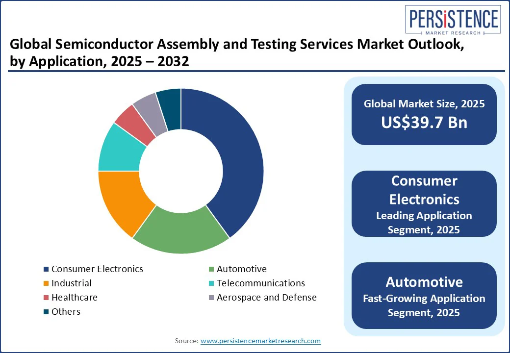
Application Insights - Consumer Electronics Lead Due to Rapid Product Upgrade Cycles and Constant Innovation
Based on applications, the market is segmented into consumer electronics, automotive, industrial, telecommunications, healthcare, aerospace & defense, and others. Among these, the consumer electronics segment is expected to hold the largest market share of 40% in 2025, driven by shipments of over a billion smartphones and tablets. This surge fuels strong demand for OSAT providers to deliver fast, high-quality packaging and testing solutions such as wafer-level packaging and flip-chip assembly. Rapid product cycles and frequent upgrades necessitate efficient, accurate semiconductor processing to meet performance standards.
The automotive sector is the fastest-growing segment, driven by the surge in electric vehicles, ADAS technologies, and the increasing use of electronics in cars. In 2024, EV sales topped 17 million units, creating a strong demand for advanced packaging and rigorous testing of automotive-grade chips. As vehicles evolve into highly connected, software-driven systems, providers are expanding capabilities to meet these needs.
Regional Insights
Asia Pacific Semiconductor Assembly and Testing Services Market Trends
The Asia Pacific region holds the largest and fastest-growing share in the global Semiconductor Assembly and Testing Services (SATS) market, accounting for nearly 60% in 2025. This growth is primarily driven by the strong presence of leading OSAT players such as ASE, JCET, ChipMOS, HANA, and UTAC, based in key countries such as China, Taiwan, South Korea, Japan, Singapore, and Malaysia. The advanced packaging and testing expertise drive the region’s growth, with ASE projecting its revenue from advanced packaging to surge from US$600 Mn in 2024 to US$1.6 Bn in 2025, fueled by AI chip demand. India is also emerging, with Tata’s TSAT plant in Assam set to start operations by mid-2025, marking the country’s first major OSAT facility.
Asia Pacific’s leadership is reinforced by its vast infrastructure, with SEMI reporting over 150 OSAT facilities in China, 130 in Taiwan, and 60+ in Southeast Asia. Many of these are equipped with cutting-edge packaging technologies such as flip-chip, fan-out wafer-level packaging (FOWLP), and 2.5D/3D integration, supporting the rising demand for AI, EV, and high-performance computing chips.
North America Semiconductor Assembly and Testing Services Market Trends
North America has emerged as the fastest-growing region, supported by large-scale government investments and a strong push to boost domestic semiconductor manufacturing and packaging capabilities. The U.S. CHIPS and Science Act, signed in 2022, has allocated over US$32 Bn by mid?2024 toward semiconductor manufacturing, packaging, and testing projects, directly supporting the development of advanced facilities across the country. Companies such as Global Foundries, Amkor Technology, and SK Hynix have announced multi?billion?dollar investments in new OSAT plants in states including New York, Arizona, and Indiana, aiming to expand capacity for high?demand technologies such as AI processors, electric vehicle chips, and 5G components.
This government?industry collaboration has created new tech hubs and research centers, with over 30 regions in the U.S. designated as semiconductor Tech Hubs, attracting billions in private capital and building local talent pipelines. The Semiconductor Industry Association (SIA) reported in 2024 that semiconductor sales in the Americas surged by 46.3% year-over-year, the highest growth rate globally, with the SATS segment playing a pivotal role due to increased demand for advanced chips in AI, data centers, and electric vehicles.
Europe Semiconductor Assembly and Testing Services Market Trends
The European semiconductor assembly and testing market has gained strategic importance, driven by strong policy measures, industrial expertise, and investment in innovation. The European Chips Act, launched in September 2023, aims to raise Europe’s global chip production share from less than 10% to 20% by 2030. It is backed by around €43?Bn (US$46.87 Bn) in public funding, supported by programs such as Horizon Europe and Digital Europe, and paired with over €100?Bn (US$115.8 Bn) in private commitments. A key focus of the Act is expanding back?end capabilities, including assembly, packaging, and testing infrastructure, to reduce reliance on Asia and secure supply chains for critical sectors such as automotive, aerospace, and industrial electronics.
Countries including the Netherlands are investing €133?Mn (US$155 Mn) into photonic chip pilot plants, while Austria is supporting an optoelectronic semiconductor site in Premstätten, demonstrating how national projects complement EU-level efforts. With strong research institutions (Imec) and companies (STMicroelectronics and ASML) leading innovation, Europe is positioning itself as a vital hub for high?value semiconductor assembly and testing.
Semiconductor Assembly and Testing Services Market Competitive Landscape
The semiconductor assembly and testing services market is highly consolidated, with major players such as ASE Technology, Amkor Technology, and JCET Group holding significant global market shares. Companies focus on expanding advanced packaging capabilities, investing in R&D, and pursuing geographic diversification to reduce reliance on overseas operations. They also emphasize strategic partnerships with fabless semiconductor companies and IDMs to secure long-term contracts.
Key Industry Developments
- In May 2025, Siemens Digital Industries Software expanded its OSAT Alliance with the inclusion of Mosaic Microsystems and NHanced Semiconductors. This initiative supports the development of assembly design kits (ADKs) using Siemens’ EDA tools to advance heterogeneous integration and secure domestic semiconductor packaging capabilities in the U.S.
- In January 2025, Micross Components acquired Integra Technologies, a U.S.-based OSAT provider specializing in high-reliability applications for military, medical, automotive, and communications sectors. Integra offers services such as die preparation, assembly, testing, and counterfeit detection through facilities in Kansas and California.
- In December 2024, Suchi Semicon inaugurated Gujarat's first Outsourced Semiconductor Assembly and Testing (OSAT) plant in Surat. With a US$100 Mn investment, the facility will initially produce 300,000 chips daily and scale up to 3 million, supporting sectors such as automotive and consumer electronics.
Companies Covered in Semiconductor Assembly and Testing Services Market
- ASE Technology Holding Co., Ltd.
- Amkor Technology, Inc.
- JCET Group Co., Ltd.
- SPIL (Siliconware Precision Industries Co., Ltd.)
- TFME (Tongfu Microelectronics Co., Ltd.)
- Unisem
- Powertech Technology Inc.
- UTAC Holdings Ltd.
- ChipMOS Technologies Inc.
- King Yuan Electronics Co., Ltd.
- Chipbond Technology Corporation
Frequently Asked Questions
The global semiconductor assembly and testing services market is projected to be valued at US$39.7 Bn in 2025.
Rising demand for advanced, miniaturized electronics is driving the need for high-performance, cost-efficient semiconductor assembly and testing services.
The semiconductor assembly and testing services market is poised to witness a CAGR of 6.7% from 2025 to 2032.
Advancements in heterogeneous integration and rising demand for semiconductor content in AI, 5G, EVs, and IoT are driving the market.
ASE Technology Holding Co., Ltd, Amkor Technology, Inc., JCET Group Co., Ltd., SPIL (Siliconware Precision Industries Co., Ltd.), TFME (Tongfu Microelectronics Co., Ltd.), Unisem, and Powertech Technology Inc. are among the leading key players.


