


- Semiconductor Materials & Components
- Semiconductor Wafer Cleaning Systems Market
Semiconductor Wafer Cleaning Systems Market Size, Share, and Growth Forecast, 2025 - 2032
Semiconductor Wafer Cleaning Systems Market by Product Type (Single Wafer Cleaners, Batch Wafer Cleaners, Single-Wafer Cryogenic Systems, Others), Technology Type (Wet Cleaning, Dry Cleaning, Plasma Cleaning, Megasonic Cleaning, Others), Application Type (Front-end Cleaning, Back-end Cleaning, Post-Deposition Cleaning, Others), End-use and Regional Analysis for 2025 - 2032
Semiconductor Wafer Cleaning Systems Market Size and Trend Analysis
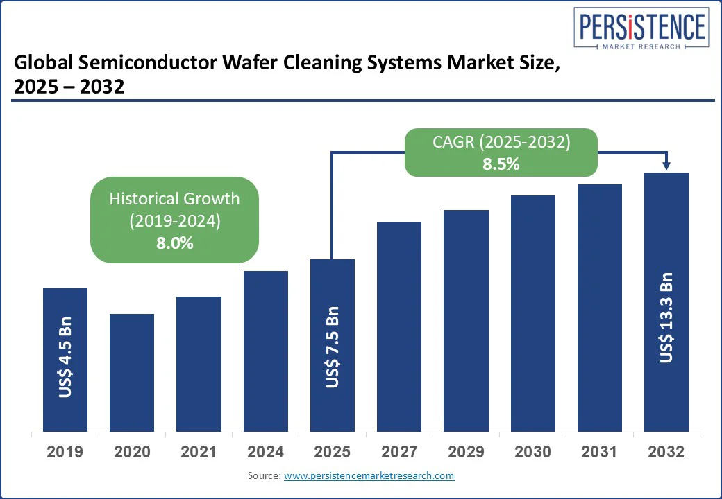
The Semiconductor Wafer Cleaning Systems Market size is likely to be valued at US$ 7.5 Bn in 2025 and is expected to reach US$ 13.3 Bn by 2032, growing at a CAGR of 8.5% from 2025 to 2032.
This growth is fueled by the increasing complexity of semiconductor devices, with node sizes shrinking below 5nm, necessitating stringent cleanliness standards. The adoption of eco-friendly cleaning solutions, automation, and AI-driven precision cleaning continues to shape the trajectory of the water cleaning system market. However, high capital costs and technical challenges in cleaning advanced materials pose restraints.
Key Industry Highlights
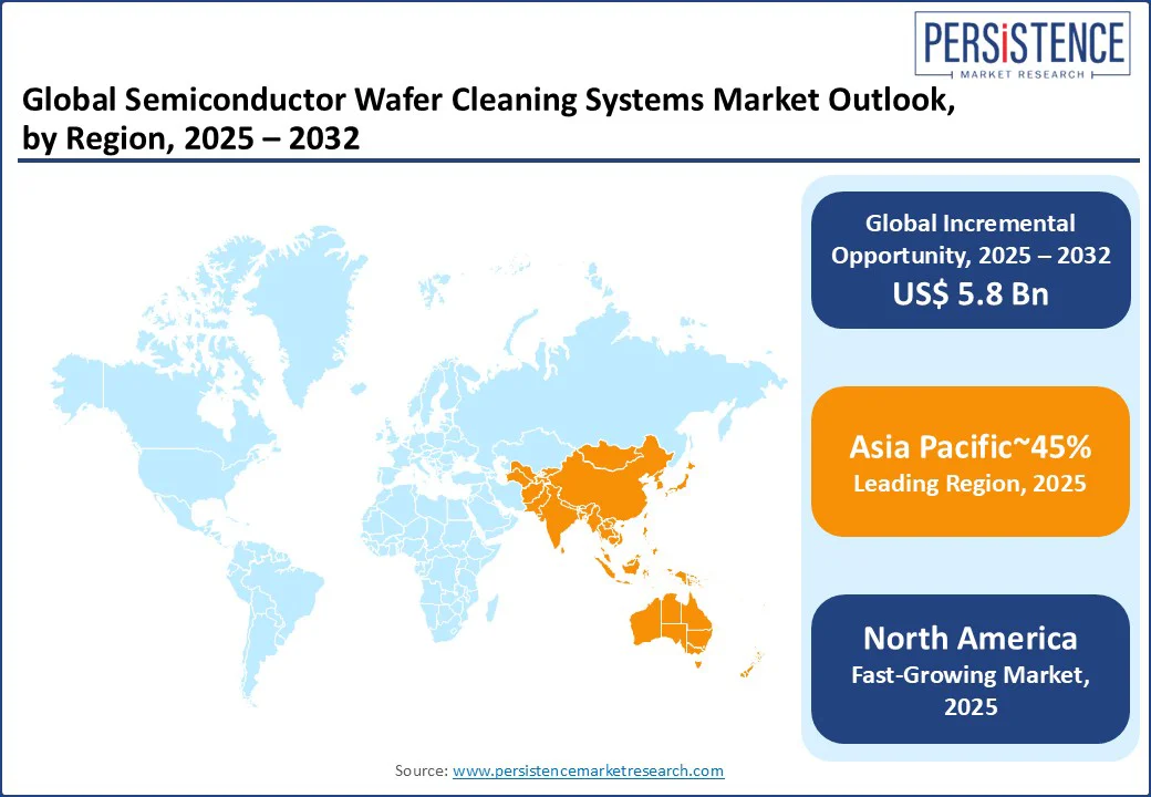
- Leading Region - Asia Pacific dominates 45% of the semiconductor wafer cleaning systems market share in 2025, supported by its leadership in global semiconductor manufacturing.
- Fastest-growing Region - North America is projected to record the fastest-growing CAGR between 2025 and 2032, driven by the U.S. CHIPS and Science Act and large-scale investments in domestic wafer fabrication plants.
- Dominant Product Type - Single Wafer Cleaners: Set to hold over 35% share in 2025, favored for their precision, uniform cleaning, and compatibility with advanced semiconductor nodes.
- Leading Technology - Wet Cleaning: Anticipated to capture 40% market share in 2025, valued for its proven cost-effectiveness and reliability in high-volume wafer production.
|
Global Market Attribute |
Key Insights |
|
Semiconductor Wafer Cleaning Systems Market Size (2025E) |
US$7.5 Bn |
|
Market Value Forecast (2032F) |
US$13.3 Bn |
|
Projected Growth (CAGR 2025 to 2032) |
8.5% |
|
Historical Market Growth (CAGR 2019 to 2024) |
8.0% |
Market Dynamics
Driver: Rising Demand for Advanced Semiconductor Devices
The semiconductor wafer cleaning systems market is experiencing robust growth due to the rising demand for advanced semiconductor devices, such as AI-driven memory, high-performance integrated circuits (ICs), MEMS, and micro-electromechanical systems.
As fabrication technologies move toward smaller process nodes, wafer surfaces become increasingly sensitive to contaminants, making advanced wafer cleaning equipment indispensable for yield improvement and device reliability.
For instance, the U.S. CHIPS and Science Act allocates over US$39 Bn to strengthen domestic semiconductor manufacturing, with funding directed toward equipment procurement, including state-of-the-art wafer cleaning systems. This initiative enables fabs to meet the stringent cleanliness requirements of next-generation chips, supporting high-performance applications in AI, 5G, and automotive electronics. Such government-backed investments are a key driver for the semiconductor wafer cleaning systems market, ensuring that manufacturers can deliver cutting-edge devices with exceptional performance and longevity.
Restraint: High Capital Investment and Maintenance Costs
The semiconductor wafer cleaning systems market faces a significant restraint due to the substantial capital investment required for advanced cleaning equipment. Cutting-edge wet cleaning modules can cost over USD 5 Mn each, while complete wafer cleaning system installation, along with facility modification, can reach tens of millions of dollars. Such high initial costs limit adoption among small and medium-sized semiconductor manufacturers, delaying equipment upgrades and production expansion.
In addition to high purchase prices, maintenance costs further increase the total cost of ownership. Routine servicing, replacement of precision components, and adherence to stringent contamination control standards contribute to elevated operational expenses. For advanced single-wafer cleaning systems required in sub-5 nm manufacturing processes, upkeep demands specialized expertise and frequent calibration, adding to long-term financial burdens. These combined capital and maintenance expenses act as a major barrier to wider adoption, constraining the overall growth potential of the semiconductor wafer cleaning systems market.
Opportunity: Adoption of Eco-friendly and Automated Cleaning Solutions
The semiconductor wafer cleaning systems market is set for significant growth through the rising adoption of eco-friendly and automated cleaning technologies. Growing environmental regulations and sustainability commitments are pushing semiconductor manufacturers to shift toward water-efficient, chemical-reducing, and low-energy cleaning processes. Eco-friendly wafer cleaning systems not only help in minimizing hazardous waste but also lower operating costs, aligning with global green manufacturing initiatives.
Automation further enhances this opportunity by improving throughput, consistency, and process reliability in wafer cleaning. AI-integrated cleaning tools and robotics-enabled handling systems reduce human error, optimize chemical usage, and ensure precise cleaning for sub-5 nm nodes.
These innovations help manufacturers meet both environmental and performance demands, making automated, eco-friendly systems a strategic investment. As industry leaders prioritize greener, smarter solutions, the semiconductor wafer cleaning systems market is expected to see accelerated adoption, driven by the dual benefits of sustainability and operational efficiency in semiconductor manufacturing.
Category-wise Analysis
Product Type Insights
Single Wafer Cleaners hold approximately 35% market share. Single wafer cleaners lead the semiconductor wafer cleaning systems market due to their ability to deliver highly precise, uniform cleaning essential for advanced sub-5 nm semiconductor nodes. These systems minimize particle contamination, improve yields, and are compatible with various wafer sizes, making them indispensable for high-performance IC manufacturing.
The Single-Wafer Cryogenic Systems segment is projected to grow at the highest CAGR, driven by its eco-friendly, chemical-free cleaning process. Utilizing cryogenic CO? snow or similar methods, these systems align with global sustainability regulations while delivering superior cleaning for sensitive wafers. Their reduced chemical usage and environmental benefits make them increasingly attractive to modern semiconductor fabs.
Technology Type Insights
Wet Cleaning dominates with approximately 40% market share. Wet cleaning remains the preferred technology in the semiconductor wafer cleaning systems market due to its effectiveness in removing particles, organic residues, and metal contaminants. It is widely used in both front-end and back-end semiconductor manufacturing processes, supporting diverse wafer materials and device types.
Plasma Cleaning is expected to grow fastest, as plasma cleaning offers a dry, damage-free method for preparing ultra-sensitive wafers. Its precision in removing organic contaminants without chemicals makes it ideal for advanced applications such as AI chips, MEMS, and 3D NAND devices. As demand for miniaturized, high-performance chips increases, plasma cleaning adoption is accelerating.
Application Type Insights
Front-End Cleaning has captured over 55% market share, and front-end cleaning dominates the semiconductor wafer cleaning systems market as it is critical for removing contaminants before photolithography, deposition, and etching steps. It directly impacts yield and device reliability in high-volume manufacturing.
The Post-Deposition Cleaning segment is witnessing the fastest growth due to the complexity of multi-layer semiconductor architectures and advanced packaging. Post-deposition cleaning ensures defect-free surfaces after thin-film or dielectric layers are applied, supporting the fabrication of next-generation memory, logic, and power devices. The rise in 3D chip designs is boosting demand for this application.
End-use Type Insights
Semiconductor Manufacturers account for over 55% market share. Semiconductor manufacturers are the largest end-use segment in the semiconductor wafer cleaning systems market due to their continuous investments in advanced wafer processing technologies and large-scale production needs.
The Research Laboratories segment is expanding rapidly as R&D in nano-electronics, quantum computing, and novel semiconductor materials intensifies. Government funding programs and partnerships between academia and industry are driving the adoption of advanced wafer cleaning systems in laboratories for prototype and experimental chip production. The focus on innovation and advanced process development fuels this growth.
Regional Insights
North America Semiconductor Wafer Cleaning Systems Market Trends
North America accounts for around 25% of the global semiconductor wafer cleaning systems market and is the fastest-growing regional segment. Growth is fueled by the expansion of domestic chip manufacturing under initiatives such as the U.S. CHIPS and Science Act, which allocates $39 Bn in incentives for semiconductor fabrication equipment, including advanced wafer cleaning systems.
Rising demand for AI processors, 5G infrastructure, and automotive electronics is driving investment in sub-5 nm and advanced packaging nodes, where precision cleaning is critical. Strategic collaborations between U.S. fabs, equipment manufacturers, and research institutes further accelerate the adoption of cutting-edge wafer cleaning technologies in the region.
Europe Semiconductor Wafer Cleaning Systems Market Trends
Europe holds a significant share in the global semiconductor wafer cleaning systems market, supported by its strong semiconductor manufacturing base and focus on high-value applications such as automotive electronics, industrial automation, and renewable energy systems. Countries such as Germany, France, and the Netherlands are home to leading semiconductor fabs and equipment suppliers, driving consistent demand for advanced wafer cleaning solutions.
The region benefits from EU initiatives such as the European Chips Act, which aims to double Europe’s global chip production share by 2030, encouraging investment in state-of-the-art fabrication equipment. Growing adoption of sub-10 nm technologies and sustainable, eco-friendly cleaning processes further boost market growth in Europe.
Asia Pacific Semiconductor Wafer Cleaning Systems Market Trends
Asia Pacific dominates the semiconductor wafer cleaning systems market with an estimated 45% market share, driven by its position as the global hub for semiconductor manufacturing. Countries such as Taiwan, South Korea, Japan, and China host leading foundries and integrated device manufacturers (IDMs), including TSMC, Samsung, and SMIC, which consistently invest in advanced wafer processing technologies.
Rapid adoption of sub-5 nm nodes, AI-driven chips, and 3D packaging fuels demand for high-precision wafer cleaning solutions. Government-backed semiconductor initiatives, such as China’s IC Industry Plan and South Korea’s K-Semiconductor Strategy, further strengthen regional growth. Strong supply chain integration and R&D investments keep the Asia Pacific at the forefront of technological advancements in wafer cleaning systems.
Competitive Landscape
The global semiconductor wafer cleaning systems market is highly competitive, led by major players such as Applied Materials, Lam Research, Tokyo Electron, SCREEN Holdings, KLA, and Shibaura Mechatronics, which focus on AI integration, automation, and eco-friendly solutions. Niche firms such as Yield Engineering Systems target specialized areas such as cryogenic cleaning. Growing adoption of plant-based chemical alternatives in adjacent markets and demand for real-time monitoring are intensifying competition, pushing companies toward continuous innovation and strategic partnerships.
Key Industry Developments
- Dec 2022 - SCREEN Holdings launched the SU-3400 single-wafer cleaning system with a 30% smaller footprint, 1,200 wafers/hour throughput, improved chemical efficiency, and 20% lower air emissions.
- Nov 2024 - ACM Research upgraded its Ultra C Tahoe tool, cutting sulfuric acid use by 75% and saving fabs up to US$ 500,000 annually while maintaining advanced cleaning performance.
Companies Covered in Semiconductor Wafer Cleaning Systems Market
- YIELD ENGINEERING SYSTEMS, INC
- TOKYO ELECTRON LIMITED
- COMPANY9
- SHIBAURA MECHATRONICS CORPORATION
- COMPANY8
- COMPANY10
- APPLIED MATERIALS, INC.
- KLA TENCOR CORP
- SCREEN HOLDINGS CO., LTD
- LAM RESEARCH CORPORATION
- Others
Frequently Asked Questions
The Semiconductor Wafer Cleaning Systems Market is projected to reach US$ 7.5 Bn in 2025.
Increasing demand for advanced semiconductors, shrinking node sizes, and government investments in fab expansions are key drivers.
The Semiconductor Wafer Cleaning Systems Market is poised to grow at a CAGR of 8.5% from 2025 to 2032.
Eco-friendly cleaning technologies and AI-integrated systems offer significant growth potential.
Applied Materials, Inc., Lam Research Corporation, Tokyo Electron Limited, SCREEN Holdings Co., Ltd., and KLA Corporation are major players.


