


- Semiconductor Materials & Components
- Semiconductor Assembly and Packaging Equipment Market
Semiconductor Assembly and Packaging Equipment Market Size, Share, and Growth Forecast, 2026 - 2033
Semiconductor Assembly and Packaging Equipment Market by Product Type (Die Bonders, Others), Application (IDMs, OSAT), End-user (Consumer Electronics, Automotive Electronics, Others), and Regional Analysis for 2026 – 2033
Semiconductor Assembly and Packaging Equipment Market Size and Trends Analysis
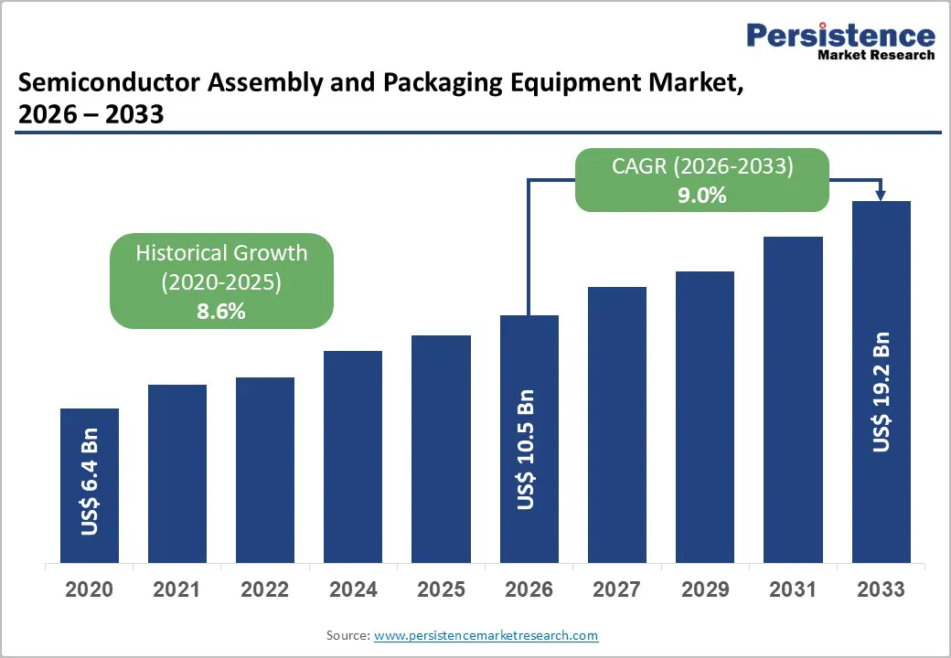
The global semiconductor assembly and packaging equipment market size is likely to be valued at US$10.5 billion in 2026, and is expected to reach US$19.2 billion by 2033, growing at a CAGR of 9.0% during the forecast period from 2026 to 2033, driven by the increasing prevalence of advanced packaging technologies, rising demand for high-performance chips in AI, 5G and automotive electronics, and advancements in die bonding and wire bonding equipment.
Growing demand for precise, high-throughput semiconductor assembly and packaging equipment, especially die bonders and flip-chip packaging systems, is accelerating adoption across applications. Advances in heterogeneous integration and fan-out wafer-level packaging are further increasing adoption by enabling improved performance and miniaturization. The increasing recognition of semiconductor assembly and packaging equipment as critical to next-generation chip production in emerging AI and EV markets remains a major driver of market growth.
Key Industry Highlights:
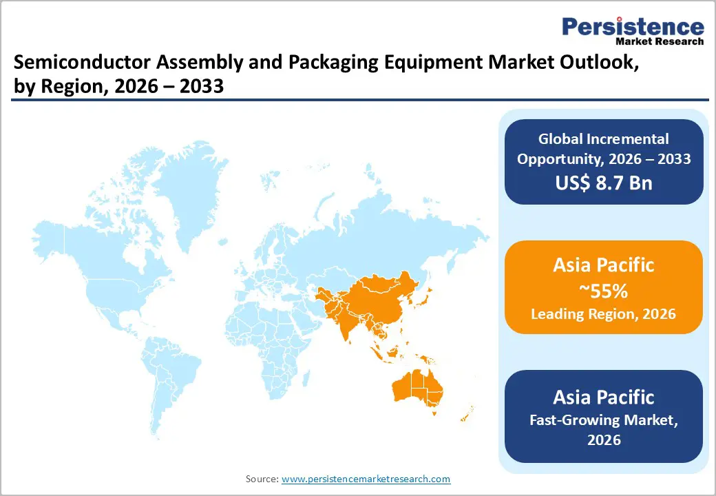
- Leading Region: Asia Pacific, anticipated to account for a 55% market share in 2026, driven by dominant OSAT capacity, massive foundry investments, and strong demand in Taiwan, China, and South Korea.
- Fastest-growing Region: Asia Pacific, fueled by rapid AI chip ramp-up, expanding EV electronics, and growing investments in advanced packaging.
- Dominant Product Type: Die Bonders, to hold approximately 40% of the market share, as they remain essential for die attach in advanced packages.
- Leading Application: OSAT, accounting for over 60% of market revenue due to outsourced assembly and test dominance.
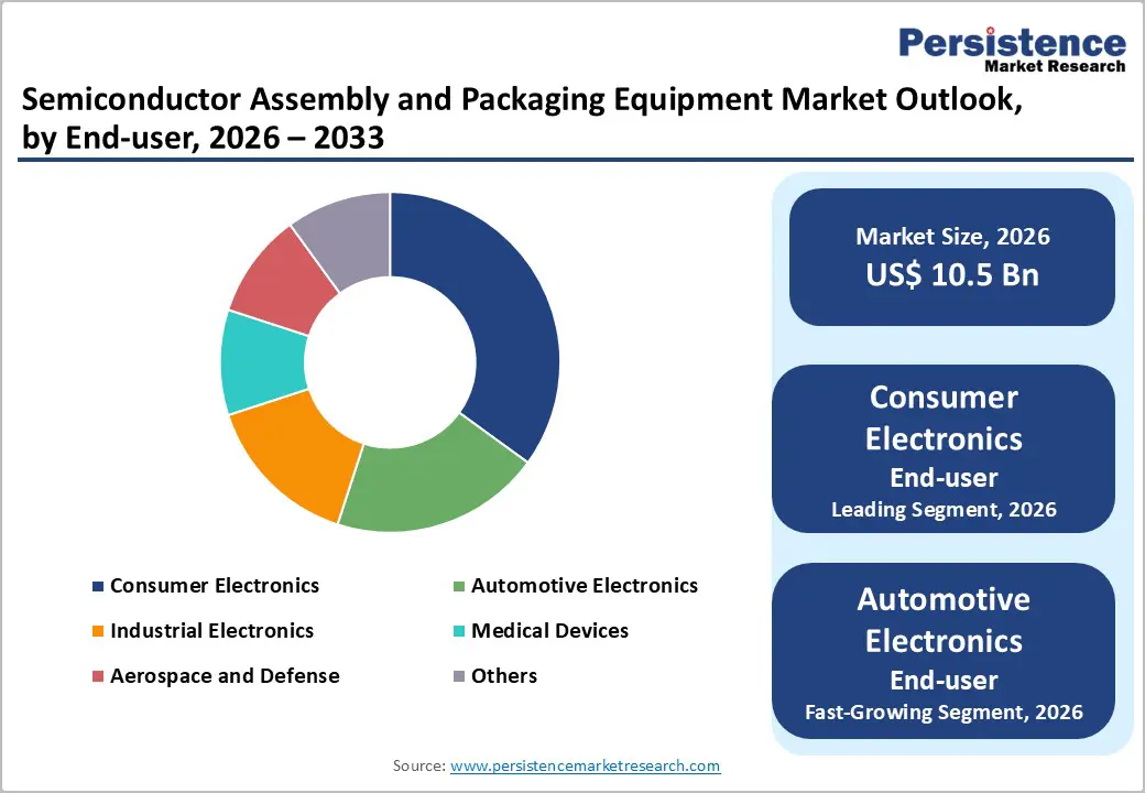
- Leading End-user: Consumer electronics, to contribute nearly 35% of the market revenue, due to smartphone, wearables, and IoT chip volumes.
| Key Insights | Details |
|---|---|
| Semiconductor Assembly and Packaging Equipment Market Size (2026E) | US$10.5 Bn |
| Market Value Forecast (2033F) | US$19.2 Bn |
| Projected Growth (CAGR 2026 to 2033) | 9.0% |
| Historical Market Growth (CAGR 2020 to 2025) | 8.6% |
Market Factors – Growth, Barriers, and Opportunity Analysis
Rising Demand for Advanced Packaging Technologies and High-Performance Chips
The rising demand for advanced packaging technologies and high-performance chips is driven by the growing complexity and performance requirements of modern electronic devices. As consumer electronics, automotive systems, artificial intelligence, and high-speed communication applications become more sophisticated, chips must deliver higher processing power, energy efficiency, and reliability. Advanced packaging solutions, such as 3D packaging, system-in-package (SiP), and fan-out wafer-level packaging (FOWLP), enable more components to be integrated into smaller form factors while improving thermal management and signal integrity. These innovations enable faster data transfer, lower latency, and improved overall device performance.
High-performance chips are also essential for emerging technologies such as 5G, cloud computing, and autonomous vehicles, where large-scale data processing and real-time decision-making are critical. Semiconductor manufacturers are investing heavily in research and development to enhance packaging density, miniaturization, and interconnect efficiency, thereby driving the adoption of these advanced chips.
5G Deployment and Telecommunication Upgrades
The deployment of 5G networks and upgrades in telecommunication infrastructure are major drivers for the semiconductor assembly and packaging equipment market. 5G technology demands high-speed data transmission, low latency, and the ability to handle massive device connectivity. To meet these requirements, advanced semiconductor devices such as radio-frequency (RF) chips, power amplifiers, and highly integrated system-on-chip (SoC) solutions are essential. These devices rely on sophisticated assembly and packaging equipment to ensure compact, high-performance, and thermally efficient designs that operate under diverse environmental conditions.
Telecommunication upgrades require faster and more reliable chips not only for mobile devices but also for base stations, network servers, and edge computing nodes. As telecom operators expand 5G infrastructure globally, demand for semiconductor manufacturing tools to support high-volume production with precision and consistency is increasing. Advanced packaging technologies, including fan-out wafer-level packaging and system-in-package (SiP), are used to integrate multiple functions into a single chip while maintaining performance and energy efficiency.
High Capital Investment Requirements
The semiconductor assembly and packaging equipment market is inherently capital-intensive due to the high cost of advanced machinery and precision tools required for chip assembly and packaging processes. These machines, including die bonders, wire bonders, flip-chip bonders, and molding systems, involve highly specialized technologies capable of handling components at the micro- and nano-scale. Acquiring a full production line often requires investments ranging from several million to tens of millions of dollars, depending on the complexity and production capacity.
Companies must consider installation, calibration, and validation expenses, which are substantial as the equipment must meet strict quality and performance standards. Maintenance and regular upgrades further add to operational costs. Small- and medium-sized players face significant barriers due to these upfront investments, which limit their ability to enter or expand in the market. The rapid pace of technological innovation in semiconductor packaging, including 3D and wafer-level packaging and advanced interconnects, forces manufacturers to periodically upgrade or replace older equipment, thereby increasing total cost of ownership.
Rapid Technological Changes and Obsolescence Risks
The industry is marked by swift technological advancements, fueled by growing demand for chips that are smaller, faster, and more energy-efficient. Innovations such as 3D packaging, wafer-level packaging, advanced interposers, and system-in-package (SiP) technologies are reshaping the industry. While these advancements enable higher performance and density, they also create a significant risk of equipment obsolescence.
Manufacturers must continuously upgrade or replace assembly and packaging machinery to stay compatible with the latest chip designs and meet stringent quality standards. Older equipment often cannot support new materials, finer pitches, or emerging packaging techniques, thereby limiting production capabilities and reducing competitiveness. This rapid turnover not only increases capital expenditure but also places financial pressure on companies to forecast future technological trends accurately.
Expansion in Heterogeneous Integration and High-Throughput Delivery Platforms
The semiconductor industry is witnessing significant growth in heterogeneous integration, a process that combines multiple types of chips and components into a single package to enhance performance, reduce size, and improve energy efficiency. This trend is driven by the increasing complexity of modern electronics, such as smartphones, data center processors, and automotive systems, which require multiple functionalities within compact form factors. Heterogeneous integration allows designers to mix logic, memory, sensors, and analog components in a single package, delivering higher performance while reducing interconnect delays and power consumption.
Semiconductor assembly and packaging equipment must adapt to high-throughput delivery platforms that can handle large volumes of diverse components quickly and accurately. Automated systems, advanced pick-and-place machines, and parallel processing tools are essential to achieve the required speed, precision, and scalability. High-throughput platforms not only accelerate production cycles but also reduce operational costs by optimizing material usage and minimizing errors during assembly.
Expansion of Data Centers and AI Applications
The rapid growth of data centers and the increasing adoption of artificial intelligence (AI) applications are creating significant opportunities in the semiconductor assembly and packaging equipment market. Data centers, which power cloud computing, online services, and enterprise IT infrastructure, require high-performance processors, memory modules, and specialized chips capable of handling massive data volumes efficiently. These advanced chips often utilize complex packaging techniques, such as multi-chip modules, 3D stacking, and system-in-package (SiP), which demand sophisticated assembly and packaging equipment.
AI applications, including machine learning, natural language processing, and computer vision, rely on specialized accelerators such as GPUs, TPUs, and AI inference chips. Manufacturing these components requires precise bonding, interconnects, and thermal management solutions, all of which increase the demand for high-throughput and high-precision packaging equipment. As AI workloads become more complex, the density and performance requirements of semiconductors increase, prompting manufacturers to adopt advanced packaging technologies that maintain speed, reliability, and thermal efficiency.
Category-wise Analysis
Product Type Insights
Die bonders are expected to lead the market, capturing around 40% of the share by 2026, owing to their essential function of precisely and reliably attaching semiconductor dies to substrates. They support a wide range of packaging types, including flip-chip, wire bonding, and wafer-level packaging, making them versatile for various applications. Their ability to handle fine-pitch dies, maintain alignment accuracy, and ensure strong mechanical and thermal connections makes them essential for high-performance chips. Growing demand for advanced packaging, miniaturized devices, and high-volume production in consumer electronics, automotive, and data center sectors further strengthens die bonders’ market dominance. BE Semiconductor Industries (Besi), a major global supplier of die-bonding equipment, has consistently captured a significant share of the die-bonding market due to its advanced bonding systems used in high-volume semiconductor packaging. Besi’s B100 die bonder is designed specifically for high-throughput and precision die attach processes, making it well-suited for applications such as automotive semiconductors and logic/memory devices where accuracy and efficiency are critical.
Packaging equipment is the fastest-growing segment, driven by the increasing complexity and performance requirements of modern semiconductor technologies. As chips become smaller, faster, and more multifunctional, advanced packaging technologies are essential to ensure reliability, thermal management, and signal integrity. Packaging equipment, which includes tools for molding, encapsulation, soldering, and substrate preparation, plays a crucial role in protecting delicate semiconductor dies while enabling high-density interconnections. Amkor Technology announced plans to build a major advanced packaging campus in Arizona. The facility, supported by significant investment and government incentives, is designed to tackle capacity constraints in high-density packaging and manage complex packaging processes for clients such as Apple and Nvidia. This project highlights the growing demand for advanced packaging equipment and services, reflecting the critical role of packaging solutions in supporting next-generation semiconductor devices.
End-user Insights
Consumer electronics are expected to dominate the market, contributing nearly 35% of revenue in 2026, propelled by the rising uptake of smart devices, wearables, and connected home technologies. Rising consumer demand for convenience, entertainment, and efficiency fuels growth, while continuous innovation in smartphones, smart TVs, and personal gadgets enhances user experience. The expanding internet penetration, affordable devices, and evolving lifestyles support widespread adoption. Manufacturers are investing in research and development to introduce feature-rich, energy-efficient products, further strengthening the segment’s market position. LG unveiled its AI-powered home robot, LG CLOiD, designed to autonomously perform household tasks and coordinate with connected appliances through its ThinQ ecosystem. This reflects a significant R&D investment in smart home robotics and integrated device control features that enhance convenience and efficiency in daily life.
Automotive electronics is the fastest-growing segment, driven by the rapid adoption of advanced driver-assistance systems (ADAS), electric vehicles (EVs), and connected-car technologies. Consumers increasingly demand enhanced safety, comfort, and infotainment features, driving manufacturers to integrate sensors, cameras, and smart control units. The shift toward electrification further accelerates growth, as EVs require sophisticated battery management systems, power electronics, and regenerative braking controls. Rising government regulations on vehicle emissions and safety standards encourage innovation in electronic components. Qualcomm, a major semiconductor company, partnered with BMW to launch Snapdragon Ride Pilot, an advanced driver-assistance system (ADAS) that enables hands-free highway driving and automated lane changes. This system debuts in BMW’s electric iX3 and will expand to many more markets by 2026, illustrating how automotive electronics, including chips and software for safety and autonomy, are becoming central to vehicle design.
Regional Insights
North America Semiconductor Assembly and Packaging Equipment Market Trends
North America growth is supported by a well-established semiconductor design landscape, robust research and development infrastructure, and strong consumer awareness of the performance and safety advantages offered by advanced electronic technologies. Manufacturing systems in the U.S. and Canada provide extensive support for packaging programs, ensuring wide accessibility of semiconductor assembly and packaging equipment across consumer electronics, automotive, and industrial populations. Increasing demand for heterogeneous integration, convenient, and easy-to-scale forms is further accelerating adoption, as these formats improve yield and reduce barriers associated with legacy tools.
Innovation in semiconductor assembly and packaging equipment, including stable hybrid bonding, improved high-throughput delivery, and targeted AI chip enhancement, is attracting significant investment from both the public and private sectors. Government initiatives and CHIPS Act campaigns continue to promote use against supply chain risks, node scaling, and emerging performance threats, creating sustained market demand. The growing focus on automotive grades and specialty uses, particularly in aerospace and other sectors, is expanding the range of target applications for semiconductor assembly and packaging equipment.
Europe Semiconductor Assembly and Packaging Equipment Market Trends
Market growth in Europe is fueled by rising recognition of performance advantages, a well-developed automotive manufacturing and engineering base, and government-backed initiatives to strengthen semiconductor development and production. Countries such as Germany, France, and the Netherlands have well-established chip frameworks that support routine packaging and encourage the adoption of innovative equipment for semiconductor assembly and packaging. These high-precision formulations are particularly appealing to automotive populations, regulatory-conscious operators, and industrial users, thereby improving yield and coverage rates.
Technological advancements in semiconductor assembly and packaging equipment, such as enhanced bonding, application-specific delivery, and improved throughput grades, are further enhancing market potential. European authorities are increasingly supporting research and trials of equipment for both routine and specialized needs, thereby strengthening market confidence. The growing emphasis on convenient, sustainable options aligns with the region’s focus on preventive supply chain resilience and on reducing import dependence. Public awareness campaigns and promotion drives are expanding reach in both urban and rural areas, while suppliers are investing in precision and novel variants to increase efficacy.
Asia Pacific Semiconductor Assembly and Packaging Equipment Market Trends
Asia-Pacific is expected to dominate and be the fastest-growing market, accounting for approximately 55% of revenue in 2026, driven by rising awareness of chip manufacturing, expanding government initiatives, and expanding application programs across the region. Countries such as China, Taiwan, South Korea, and India are actively promoting equipment campaigns to address advanced packaging growth and emerging AI needs. Semiconductor assembly and packaging equipment is particularly attractive in these regions due to its high-throughput administration, ease of scaling, and suitability for large-scale OSAT drives in both urban and rural populations.
Technological advancements are enabling the development of stable, effective, and easy-to-deploy semiconductor assembly and packaging equipment that can withstand challenging cleanroom conditions and minimize yield dependence. These innovations are critical for reaching remote facilities and improving the overall chip coverage. Growing demand for consumer electronics, automotive electronics, and industrial applications is contributing to market expansion. Public-private partnerships, increased semiconductor expenditure, and rising investment in packaging research and manufacturing capacity are further accelerating growth. The convenience of equipment delivery, combined with improved precision and reduced risk of defects, positions semiconductor assembly and packaging equipment as a preferred choice.
Competitive Landscape
The global semiconductor assembly and packaging equipment market features competition between established leaders and emerging precision suppliers. In North America and Europe, Kulicke and Soffa Industries and ASM International lead through strong R&D, distribution networks, and foundry ties, bolstered by innovative die bonding and hybrid programs. In Asia Pacific, ASMPT advances with localized solutions, enhancing accessibility. High-throughput delivery boosts yield, cuts cycle-time risks, and enables mass integrations across regions. Strategic partnerships, collaborations, and acquisitions merge expertise, expand portfolios, and speed commercialization. Advanced packaging formulations solve density issues, aiding penetration in AI-focused areas.
Key Industry Developments
- In December 2025, Suchi Semicon launched advanced QFN and power packaging solutions, expanding its semiconductor packaging portfolio to support high-performance and power-efficient electronic applications and meet growing demand across the automotive, industrial, and consumer electronics sectors.
- In October 2025, Amkor Technology announced a major advanced packaging campus project in Arizona, backed by significant investment and government incentives, to expand capacity for high-density and complex packaging and to support client demand from companies such as Apple and Nvidia, underscoring strong demand for packaging equipment and services.
- In September 2025, LCY Chemical Corp. announced the launch of LCY Advanced Formulations, showcasing key technologies and sustainability strengths at the SEMICON 2025 Heterogeneous Integration Global Summit (HIGS). The company developed the advanced formulations to support high-integration and high-precision advanced packaging applications. It emphasized superior performance across various uses, high throughput, and low chemical consumption, all designed to reduce the total cost of ownership.
Companies Covered in Semiconductor Assembly and Packaging Equipment Market
- ASMPT
- Kulicke and Soffa Industries, Inc.
- Besi
- TOWA Corporation
- SHINKAWA Electric Co., Ltd.
- Hana Micron
- SUSS MicroTec SE
- ASM International
- Disco Corporation
- Advantest Corporation
- Tokyo Electron Limited
- Amkor Technology
- Screen Holdings Co. Ltd
- ROHM Co., Ltd.
- NAURA Technology Group Co., Ltd.
Frequently Asked Questions
The global semiconductor assembly and packaging equipment market is projected to reach US$10.5 billion in 2026.
The rising prevalence of advanced packaging technologies and demand for high-performance chips are key drivers.
The semiconductor assembly and packaging equipment market is poised to witness a CAGR of 9.0% from 2026 to 2033.
Advancements in heterogeneous integration and high-throughput delivery platforms are key opportunities.
ASMPT, Kulicke and Soffa Industries, Inc., Besi, ASM International, and TOWA Corporation are the key players.


