


- Smart Packaging
- Advanced Chip Packaging Market
Advanced Chip Packaging Market Size, Share, and Growth Forecast, 2026 – 2033
Advanced Chip Packaging Market by Product Type (Flip-Chip, Fan-Out WLP, System-in-Package (SiP) Solutions, Fan-In WLP, 2.5D Packaging and 3D Packaging), Application (Consumer Electronics, Automotive, Others), and Regional Analysis for 2026 – 2033
Advanced Chip Packaging Market Size and Trends Analysis
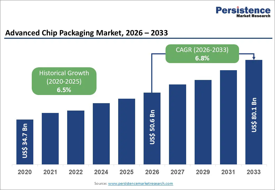
The global advanced chip packaging market size is likely to be valued at US$50.6 billion in 2026 and is expected to reach US$80.1 billion by 2033, growing at a CAGR of 6.8% during the forecast period from 2026 to 2033, driven by rising demand for high-performance computing, AI accelerators, and miniaturized consumer electronics, alongside increasing adoption in the automotive sector, where electric vehicles (EVs) and ADAS require thermally robust and high-density semiconductor modules. The growth is supported by the proliferation of 5G networks, which require highly integrated packaging solutions for RF and high-speed signal processing. Increasing adoption of system-in-package (SiP) and fan-out wafer-level packaging (FOWLP) technologies is enhancing device performance while reducing form factor. Rising demand from consumer electronics such as smartphones, tablets, and wearables continues to drive market expansion.
Key Industry Highlights:
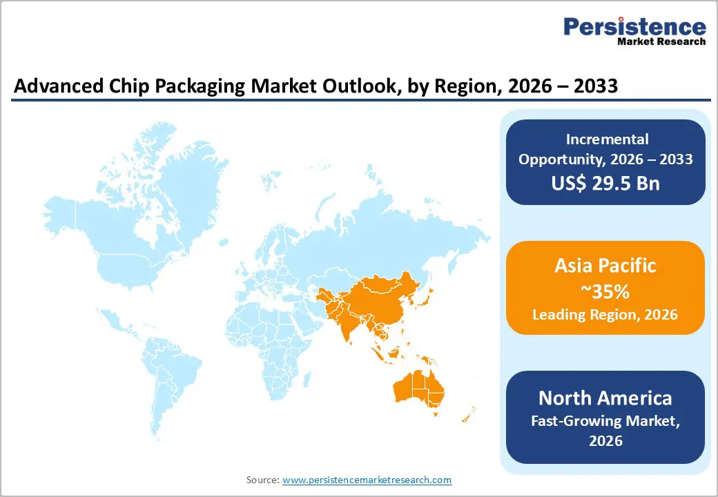
- Leading Region: Asia Pacific is anticipated to be the leading region, accounting for a market share of 35% in 2026, driven by strong semiconductor manufacturing capabilities, cost advantages, rapid 5G adoption, growth in consumer electronics, and increasing automotive and industrial demand.
- Fastest-growing Region: North America is likely to be the fastest-growing region, supported by the creation of helpful incentives to produce semiconductors (CHIPS) Act investments, AI packaging innovation, automotive electrification, regulatory incentives, and a strong semiconductor ecosystem.
- Leading Product Type: The flip-chip segment is projected to represent the leading product type in 2026, accounting for 28% of the revenue share, driven by superior electrical performance, widespread adoption in high-performance computing, GPUs, and miniaturized consumer electronics.
- Leading Application: The consumer electronics segment is expected to be the leading application type, accounting for over 35% of the revenue share in 2026, driven by the adoption of smartphones, wearables, tablets, and miniaturized packaging solutions.
| Global Market Attributes; | Key Insights; |
|---|---|
| Advanced Chip Packaging Market Size (2026E) | US$50.6 Bn |
| Market Value Forecast (2033F) | US$80.1 Bn |
| Projected Growth (CAGR 2026 to 2033) | 6.8% |
| Historical Market Growth (CAGR 2020 to 2025) | 6.5% |
Market Factors – Growth, Barriers, and Opportunity Analysis
Technological Advancements in Semiconductor Integration
Traditional scaling via Moore’s Law is reaching physical and economic limits, prompting the industry to adopt new back end solutions that enhance performance and integration without solely relying on shrinking transistor geometries. Advanced packaging technologies such as system in package (SiP), fan out wafer level packaging (FOWLP), 2.5D and 3D packaging, and heterogeneous integration enable multiple dies such as processors, memory, sensors, and RF components to be combined into a single compact package, improving electrical performance, reducing power consumption, and supporting miniaturization trends in mobile, IoT, and wearable devices.
Techniques such as through silicon vias (TSVs), hybrid bonding, and high density interconnects facilitate vertical and lateral connections between chips, enhancing signal integrity and data throughput while reducing latency. These interconnection advancements are essential for memory intensive applications and high bandwidth memory (HBM) systems used in AI, networking, and data centers. Industry momentum is amplified by advances in design automation, machine learning assisted manufacturing, and novel substrate materials that support finer pitches and improved thermal management. The adoption of advanced packaging is broadening beyond consumer electronics to automotive, aerospace, and industrial sectors, where reliability and multifunctionality are paramount.
Limited Skilled Workforce
The technologies involved require highly specialized expertise across design, assembly, testing, and integration of multi-die packages. Advanced packaging techniques demand precision at microscopic scales, and an in-depth understanding of semiconductor physics, thermal management, and high-density interconnect technologies. The shortage of trained engineers and technicians constrains the ability of Original Equipment Manufacturers (OEMs) and OSAT (Outsourced Semiconductor Assembly and Test) providers to scale operations effectively, particularly in regions experiencing rapid market growth, such as Asia Pacific and North America. Onboarding and training new talent in cutting-edge packaging processes requires significant investments in time and resources, which can slow production timelines and impact market responsiveness.
The shortage of skilled labor affects innovation and research within the sector, as advanced packaging relies heavily on continuous R&D to meet rising demands for miniaturization, power efficiency, and high-bandwidth memory integration. The limited availability of experts in through-silicon vias (TSVs), hybrid bonding, and high-density interconnects reduces the speed at which new packaging technologies can be commercialized. Countries investing in semiconductor growth initiatives, such as the U.S. CHIPS Act and India’s semiconductor mission, also face the challenge of developing a qualified workforce to support emerging fabs and OSAT operations.
Emergence of AI and Edge Computing Applications
Technologies demand high computational performance, low latency, and energy efficiency within compact form factors. AI workloads such as machine learning inference, computer vision, and natural language processing require advanced integration of processors, memory, and accelerators, which is increasingly enabled through 2.5D and 3D packaging, fan-out wafer-level packaging (FOWLP), and system-in-package (SiP) solutions. These packaging technologies allow closer proximity of logic and memory, improving bandwidth and reducing signal delay, which is critical for real-time AI processing at the edge. Edge computing applications in smart devices, industrial automation, and autonomous systems accelerate adoption, as they rely on localized data processing to minimize dependence on cloud infrastructure.
The rapid deployment of edge AI across sectors such as automotive, healthcare, manufacturing, and smart cities is driving demand for heterogeneous integration and chiplet-based architectures. Advanced chip packaging enables the integration of CPUs, GPUs, AI accelerators, sensors, and connectivity components within a single package, reducing system size while enhancing performance. This capability is particularly important for applications such as advanced driver-assistance systems (ADAS), robotics, and 5G base stations, where real-time decision-making and data processing are essential. The growing adoption of AI inference at the edge also increases demand for high-bandwidth memory and efficient power delivery, further strengthening the role of advanced packaging technologies.
Category-wise Analysis
Product Type Insights
The flip-chip is expected to lead the market, accounting for approximately 28% of revenue in 2026, driven by its strong performance characteristics and widespread adoption across high-end semiconductor applications. This packaging technology enables shorter interconnect paths, improved signal integrity, and efficient power delivery, making it highly suitable for advanced processors and graphics-intensive workloads. Flip-chip packaging also enables efficient heat dissipation, which is critical for chips running at higher power levels. For instance, it is widely used in high-performance processors for data centers and gaming systems, where the technology helps manage complex workloads more effectively.
Fan-out wafer-level packaging (WLP) is likely to represent the fastest-growing segment in 2026, supported by its ability to deliver high performance in ultra-thin and compact form factors. Fan-Out WLP enables greater I/O density and improved electrical performance without the need for traditional substrates, making it highly suitable for next-generation consumer electronics and mobile devices. The technology improves signal integrity, reduces power consumption, and enhances thermal efficiency, key requirements for advanced processors and high-performance connectivity solutions. For instance, its growing use in smartphones allows for thinner device designs while combining multiple functional components into a single, compact package.
Application Insights
The consumer electronics segment is projected to lead the market, capturing around 35% of the revenue share in 2026, supported by continuous innovation in smart devices and personal electronics. Advanced packaging technologies enable compact designs, improved power efficiency, and enhanced functionality, which are essential for modern smartphones, wearables, and computing devices. The segment benefits from high-volume production cycles and rapid product refresh rates, driving sustained demand for efficient and scalable packaging solutions. For example, the integration of system-in-package and fan-out technologies in smartphones where multiple components, such as processors, memory, and connectivity modules, are combined within a single compact package.
The automotive segment is likely to be the fastest-growing application, driven by the increasing integration of electronics into modern vehicles. Advanced packaging solutions are essential for meeting the stringent reliability, durability, and thermal requirements of automotive environments. The shift toward EVs and intelligent driver assistance systems is accelerating demand for high-density, high-performance semiconductor modules. For example, the use of advanced packaging in automotive control units, where multiple chips are integrated to support real-time processing and safety-critical functions. These solutions enable efficient power management and robust performance under extreme operating conditions.

Regional Insights
North America Advanced Chip Packaging Market Trends
North America is expected to be the fastest-growing region in advanced chip packaging, fueled by rising demand across AI, high-performance computing (HPC), telecommunications, and automotive applications. A key trend is the growing adoption of 2.5D and 3D packaging technologies, which offer shorter interconnects, lower latency, and higher bandwidth, capabilities that are essential for data centers and edge computing platforms supporting next-generation AI workloads. These advanced integration approaches also enable larger memory stacks, delivering more efficient processing within compact form factors. For instance, Intel’s Foveros 3D stacking technology highlights how U.S.-led innovation in advanced packaging is driving improved performance and energy efficiency for AI and HPC chips, reinforcing the region’s leadership in packaging technology development.
In North America, there is a strong emphasis on expanding domestic packaging capacity and enhancing supply chain resilience to reduce dependence on overseas facilities and mitigate geopolitical risks. Investments in new advanced packaging plants, along with the growth of existing sites, are contributing to the development of more comprehensive, end-to-end semiconductor manufacturing ecosystems within the region. For instance, Amkor Technology’s groundbreaking of a large advanced packaging campus in Arizona exemplifies efforts to strengthen U.S.-based packaging capabilities by closely integrating front-end wafer fabrication with back-end advanced packaging operations. The facility is designed to support complex packaging for AI accelerators, high-bandwidth memory, and other high-performance applications, helping to alleviate longstanding supply chain constraints in the U.S.
Europe Advanced Chip Packaging Market Trends
Europe is likely to be a significant market for advanced chip packaging in 2026, due to growing demand for high-reliability semiconductor solutions and strategic regional investments in technology development. European manufacturers are leveraging their strengths in precision engineering and niche packaging capabilities to serve high-value applications that demand robust electrical performance and thermal efficiency. For example, the emphasis on automotive-grade and industrial packaging solutions requires stringent reliability standards and drives adoption of advanced packaging techniques across vehicle control units and power modules.
Another key trend in the market is the shift toward sustainable and energy-efficient semiconductor manufacturing, as well as efforts to expand local capacity and reduce dependency on external suppliers. This drive is supported by strong investments from regional players and research collaborations to accelerate the commercialization of next-generation packaging processes, including heterogeneous integration and vertical stacking techniques. Demand for energy-efficient designs is particularly pronounced in electric vehicle and data infrastructure applications, where advanced packaging helps optimize power delivery and heat dissipation. European companies are also participating in international partnerships and ecosystem initiatives to advance packaging innovation and competitiveness. STMicroelectronics demonstrates this trend through investments in panel-level packaging pilot production capacity in France, aiming to enhance automation and packaging efficiency for next-generation semiconductors.
Asia Pacific Advanced Chip Packaging Market Trends
The Asia Pacific region is anticipated to be the leading region, accounting for a market share of 35% in 2026, driven by the region’s strong semiconductor ecosystem, high-volume manufacturing capabilities, and rising demand for performance-oriented applications such as AI, 5G, and EV electronics. Rapid growth in AI-driven data centers and mobile devices has pushed manufacturers to integrate heterogeneous components into single packages, enhancing performance and reducing power consumption. For example, Taiwan Semiconductor Manufacturing Company (TSMC), continues to expand its advanced packaging capacity, particularly CoWoS and chiplet-based solutions, to meet the rising demand from partners and deliver better performance for AI accelerators and networking chips.
Asia Pacific is experiencing an increasing diversification of manufacturing hubs outside of traditional locations, underpinned by cost efficiencies and strategic investment incentives. Emerging destinations such as India, Vietnam, and Malaysia are attracting semiconductor assembly and packaging activities due to competitive labor costs, favorable policy frameworks, and expanding local demand for smart electronics and automotive systems. For example, Amkor Technology has been expanding its presence in key Asia Pacific markets with enhanced fan-out and multi-chip packaging facilities, aligning capacity with growing regional demand for high-density integration across consumer, automotive, and industrial applications.
Competitive Landscape
The global advanced chip packaging market exhibits a moderately fragmented structure, driven by a mix of integrated device manufacturers (IDMs), foundries, and specialized outsourced semiconductor assembly and test (OSAT) providers, all competing to deliver proprietary and high-performance packaging solutions. This competitive structure reflects both consolidation around core technologies and ongoing specialization, with players seeking to balance scale, innovation, and regional capacity expansion to serve evolving end-use segments from consumer electronics to automotive and industrial markets.
With key leaders including TSMC, Intel, Samsung Electronics Co. Ltd., ASE Group, Amkor Technology, SK Hynix, and Siliconware Precision Industries (SPIL), companies are intensifying investments in advanced packaging R&D, strategic alliances, and capacity build-outs to secure market share and technology leadership. These players compete through differentiated technology platforms, strategic partnerships, and value-added services that enhance performance, reliability, and integration density for complex semiconductor designs.
Key Industry Developments:
- In January 2026, South Korean chip packaging equipment makers significantly intensified their push into the global advanced chip packaging market, aiming to challenge long-established international leaders as AI-driven semiconductor demand accelerates. Korean toolmakers are increasingly focusing on advanced packaging technologies such as 2.5D/3D integration, fan-out wafer-level packaging, and hybrid bonding, which are critical for high-performance AI and data-center chips. This strategic shift is supported by strong domestic semiconductor manufacturing capabilities and close collaboration with leading Korean chipmakers, enabling faster equipment validation and commercialization.
- In January 2026, Paras Defence & Space Technologies Ltd (PDST) formally entered the advanced chip packaging market with the launch of its subsidiary, Paras Semiconductor Pvt. Ltd., marking a strategic expansion into India’s semiconductor value chain. The company announced plans to establish an Outsourced Semiconductor Assembly and Test (OSAT) facility focused on advanced, heterogeneous, and 3D packaging technologies, with a strong emphasis on chiplet integration and system-in-package (SiP) solutions. This facility will support the assembly, packaging, and testing of semiconductor devices, particularly for optical and opto-electronic systems, bridging the gap between chip fabrication and final system integration.
- In March 2025, Taiwan Semiconductor Manufacturing Company (TSMC) announced a landmark expansion of its U.S. footprint, committing an additional US$100 billion to advanced semiconductor manufacturing and packaging operations in Arizona, raising its total planned U.S. investment to US$165 billion. The expansion includes three new fabrication plants, two advanced chip packaging facilities, and a major R&D center, underscoring the growing strategic importance of advanced packaging technologies alongside leading-edge wafer fabrication. TSMC stated that rising demand for AI-driven computing, high-performance processors, and next-generation applications is a key driver behind the investment.
Companies Covered in Advanced Chip Packaging Market
- Intel Corporation
- Taiwan Semiconductor Manufacturing Company Limited (TSMC)
- Advanced Micro Devices Inc. (AMD)
- Samsung Electronics Co. Ltd.
- Amkor Technology, Inc.
- ASE Group (Advanced Semiconductor Engineering Inc.)
- Qualcomm Technologies Inc. (a subsidiary of Qualcomm Incorporated)
- SK Hynix Inc.
- Siliconware Precision Industries Co. Ltd. (SPIL)
- Texas Instruments Incorporated (TI)
Frequently Asked Questions
The global advanced chip packaging market is projected to reach US$50.6 billion in 2026.
The advanced chip packaging market is driven by rising demand for high-performance computing, AI, and 5G applications, increasing chip miniaturization, and the need for higher bandwidth, power efficiency, and heterogeneous integration in next-generation semiconductor devices.
The advanced chip packaging market is expected to grow at a CAGR of 6.8% from 2026 to 2033.
Key market opportunities in the advanced chip packaging market include the rapid growth of AI and edge computing, increasing adoption of chiplet and heterogeneous integration architectures, expansion of electric vehicles and ADAS, and rising investments in advanced packaging facilities across Asia Pacific, North America, and Europe.
Intel Corporation, Taiwan Semiconductor Manufacturing Company Limited (TSMC), and Advanced Micro Devices Inc. are the leading players.


