


- Smart Packaging
- Fan-Out Wafer Level Packaging Market
Fan-Out Wafer Level Packaging Market Size, Share, Trends, Growth, Regional Forecasts 2026 - 2033
Fan-Out Wafer Level Packaging Market by Product Type (Standard Fan-Out Packaging, High-Density Fan-Out Packaging, Core Fan-Out Packaging, Others), Application (CMOS Image Sensor, Wireless Connection, Logic and Memory Integrated Circuits, MEMS and Sensors, Analog and Hybrid Integrated Circuits, Others), and Region Analysis for 2026 - 2033
Fan-Out Wafer Level Packaging Market Trends & Analysis
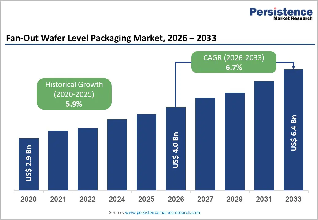
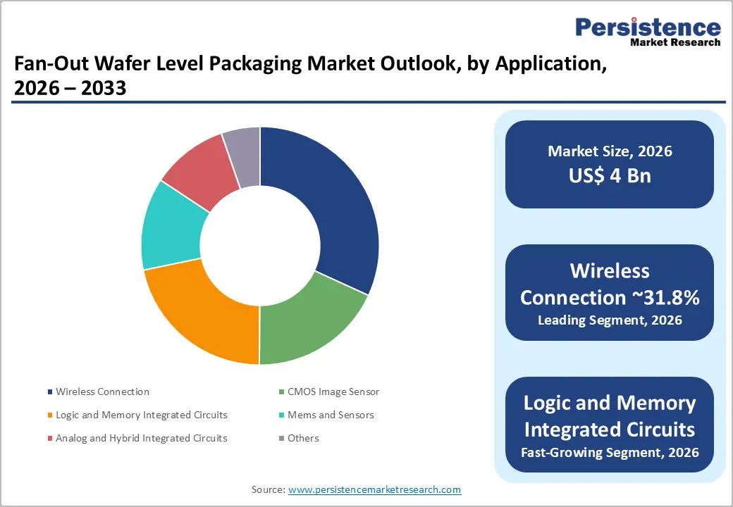
The global fan-out wafer level packaging market size is projected at US$ 4.0 billion in 2026 and is projected to reach US$ 6.4 billion by 2033, growing at a CAGR of 6.7% between 2026 and 2033. AI accelerator heterogeneous integration, 5G RF front-end module miniaturization, and automotive ADAS radar adoption are primary demand drivers. Semiconductor industry investments in advanced packaging as a Moore's Law continuation strategy, with TSMC, ASE, and Amkor collectively holding ~65% global market share, sustain commercialization momentum across mobile, data center, and automotive application verticals.
Key Industry Highlights:
- Leading Product Type: Standard Fan-Out Packaging leads at 38.7% share (~US$ 1.56 Bn); Core Fan-Out Packaging grows fastest at 12% CAGR, driven by wearable, IoT, automotive sensor, and medical device miniaturized packaging design-win expansion.
- Leading Application: Wireless connection leads at 31.8% share (~US$ 1.28 Bn); Logic and Memory ICs are likely to reach fast-growth, driven by AI accelerator heterogeneous chiplet co-packaging and HBM memory integration procurement globally.
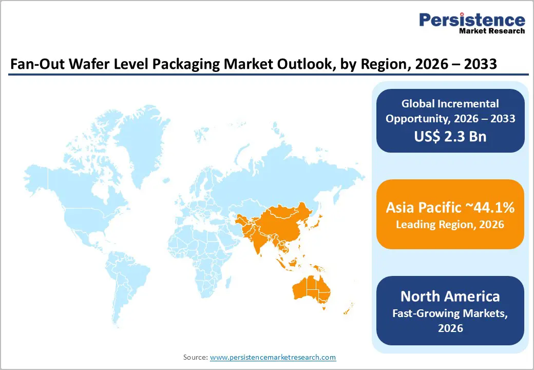
- Regional Leader: Asia Pacific leads at ~48% share in 2026. China holds US$ 725.7 Mn and India US$ 206.4 million, anchored by JCET foundry capacity and India Semiconductor Mission investment programs.
- North America & Europe: North America is likely to register 28.4% share in 2026, driven by CHIPS Act NAPMP; Europe is likely to experience a leading CAGR with Germany at US$ 275 Mn anchored by Infineon automotive FOWLP and EU Chips Act funding.
- Strategic Milestone: Amkor's US$ 2 Bn Arizona FOWLP facility inauguration (March 2025) and TSMC's US$ 40 Bn Arizona Fab 21 FOWLP production ramp signal structural North American FOWLP supply chain localization as the defining 2025–2030 competitive repositioning theme globally.
Market Dynamics Analysis
Drivers - 5G Semiconductor Proliferation and RF Front-End Module Miniaturization Driving Fan-out Wafer Level Packaging Adoption
Global 5G base station deployments exceeded 3.5 million active sites worldwide by end-2024 (GSMA Intelligence), with 5G millimeter-wave (mmWave) RF front-end modules requiring ultra-thin, high-I/O semiconductor packages that FOWLP uniquely enables at competitive cost structures versus silicon interposer-based 2.5D/3D alternatives.
FOWLP's reconstituted wafer approach allows antenna-in-package (AiP), RF transceivers, and power management ICs to co-integrate within sub-0.8 mm package profiles, critical for 5G smartphone baseband modules, driving Qualcomm and MediaTek 5G chipset supply chain FOWLP procurement volumes across TSMC, ASE, and Amkor foundry capacity globally through 2033.
The GSMA projects global 5G connections to reach 5.9 billion by 2030, expanding the RF front-end semiconductor packaging addressable market by an estimated US$ 2.1 Bn in incremental FOWLP procurement annually through 2030. Fan-out wafer level packaging eliminates conventional substrate layers required by flip-chip BGA packages, reducing parasitic losses, shortening interconnect lengths, and improving signal integrity at mmWave frequencies.
AI and High-Performance Computing Chiplet Integration Accelerating High-Density FOWLP Demand
AI inference and training semiconductor architectures, requiring heterogeneous integration of processors, HBM memory stacks, and high-bandwidth interconnects, are driving High-Density Fan-Out Packaging adoption within data center GPU, AI accelerator, and network processing unit (NPU) supply chains. Infineon's 77 GHz automotive radar modules utilize FOWLP to achieve 0.8 mm package height with 60% improved thermal cycling performance over QFN packaging, establishing FOWLP as the precision packaging benchmark across automotive and HPC semiconductor design programs globally.
The global AI semiconductor market, valued at US$ 67.1 Bn in 2024 and projected at US$ 251.4 Bn by 2030 (IDC), directly expands FOWLP addressable procurement volumes as AI chiplet heterogeneous integration mandates multi-die co-packaging solutions that FOWLP and Fan-Out Panel-Level Packaging (FOPLP) architectures best enable at scale. TSMC's Integrated Fan-Out (InFO) and CoWoS packaging platforms, anchoring Apple A-series, NVIDIA H100, and AMD MI300X supply chains, demonstrate FOWLP's established commercial role in the world's highest-value semiconductor packaging procurement programs.
Restraints - Advanced Lithography Equipment Supply Chain Constraints Limiting FOWLP Capacity Expansion
FOWLP capacity expansion requires advanced lithography tools, including ASML's EUV systems priced at US$ 150–350 Mn per unit, facing 12–18-month lead times that prevent rapid FOWLP foundry capacity scaling in response to demand surges from 5G, AI, and automotive semiconductor customers. SEMI reported global semiconductor equipment lead times averaging 20 weeks in 2024, with advanced packaging lithography tooling representing the most constrained segment, limiting FOWLP capacity expansion rates to 8–12% annually across TSMC, ASE, and Amkor global foundry networks through 2026.
Geopolitical Semiconductor Export Controls Creating FOWLP Supply Chain Fragmentation Risk
U.S. Commerce Department BIS advanced semiconductor export controls, expanding restrictions on 14nm-and-below logic chips and advanced packaging equipment exports to China in October 2023 and January 2025, directly constrain FOWLP technology transfer and capacity investment in China-based packaging foundries. JCET and SMIC's China-based FOWLP operations face technology access barriers under BIS Entity List controls, with 22% of global FOWLP capacity concentrated in China facing long-term strategic fragmentation risk as U.S. and allied export control regimes broaden advanced packaging technology restrictions through 2033.
Opportunities - Automotive Radar and ADAS Sensor FOWLP Adoption Across Electric Vehicle Proliferation
Global electric vehicle sales surpassed 17.1 million units in 2024 (IEA Global EV Outlook 2025), with each EV incorporating 25–40 ADAS semiconductor packages requiring radar, LiDAR signal processing, and functional safety-certified packaging solutions where FOWLP's thermal performance and ultra-thin profile deliver critical design advantages over conventional QFN alternatives. Infineon's 77 GHz radar module utilizing FOWLP packaging, achieving 0.8 mm height with -40°C to 150°C thermal stability, validates the automotive-grade qualification pathway for FOWLP at Tier-1 automotive supplier procurement scale.
The automotive semiconductor packaging market is projected to reach a leading CAGR as FOWLP-qualified automotive packages represent the highest-specification, highest-margin sub-segment within this addressable market. EV battery management systems, domain controller ECUs, and V2X communication modules each represent additional FOWLP design-win opportunities beyond ADAS radar, establishing automotive electronics as a durable, policy-supported FOWLP demand expansion pathway through 2033 across all major EV manufacturing geographies globally.
India Semiconductor Mission and Southeast Asia Foundry Diversification: Creating New FOWLP Capacity Investment Hubs
India's US$ 10 Bn Semiconductor Mission, approving Tata Electronics' US$ 11 Bn semiconductor fabrication plant in Gujarat and Micron's US$ 825 Mn assembly and test facility in Sanand, establishes India as an emerging FOWLP advanced packaging capacity investment destination outside the Taiwan-Korea-China concentration zone. India's FOWLP market at US$ 206.4 Mn in 2026 is positioned for accelerated growth as domestic semiconductor policy incentives and foreign direct investment programs reduce geopolitical supply chain concentration risk for global fabless semiconductor customers requiring FOWLP packaging services.
Vietnam, Malaysia, and Thailand, hosting Intel, Intel Penang, and Western Digital advanced packaging facilities, are expanding FOWLP-compatible substrate and assembly capacity through US$ 3.2 Bn in committed semiconductor facility investments through 2026 (SEMI SEA), creating structurally diversified regional FOWLP supply alternatives that reduce Taiwan-concentration risk for multinational semiconductor OEM procurement programs globally through 2033.
Category-wise Analysis
Product Type Insights
Standard Fan-Out Packaging leads the product type segment with a 38.7% share in 2026, estimated at approximately US$ 1.56 Bn, anchored by its proven high-volume manufacturing maturity across TSMC InFO, ASE FoCoS, and Amkor SWIFT platforms that serve the world's highest-volume mobile application processor, baseband, and power management IC packaging supply chains.
Standard FOWLP's cost-per-unit advantage over High-Density and Core variants, combined with established design-rule compatibility across Qualcomm, Apple, and MediaTek mobile chipset ecosystems, sustains its volume leadership. While High-Density FOWLP is growing faster, Standard FOWLP's manufacturing scale dominance at 200-I/O-and-below mobile chip tiers maintains segment leadership through 2033 without material share displacement risk at volume tier.
Core Fan-Out Packaging is the fastest-growing product type. Core FOWLP's embedded die technology enabling ultra-thin wearable device, IoT sensor, and implantable medical package profiles, combined with emerging automotive and industrial sensor applications requiring miniaturized hermetic packaging, is driving its accelerating design-win momentum beyond conventional mobile consumer electronics volumes through 2033.
Application Insights
Wireless connection leads the application segment with a 31.8% market share in 2026, estimated at approximately US$ 1.28 Bn, driven by 5G RF front-end modules, Wi-Fi 6E/7 combo chips, and Bluetooth SoC packages across smartphone, laptop, and IoT device supply chains where FOWLP's antenna-in-package integration and high-I/O density at sub-millimeter profiles deliver unmatched performance-per-area efficiency.
Wireless Connection's dominance reflects FOWLP's foundational role in enabling 5G mmWave AiP designs, a design requirement no alternative packaging technology currently matches at comparable cost and volume scale across Tier-1 OEM wireless semiconductor supply programs. CMOS Image Sensor and MEMS and Sensors segments are growing but remain volume-constrained by application-specific design cycles compared to wireless connection's mass-market volume procurement scale.
Logic and Memory Integrated Circuits is the fastest-growing application at 9.5% CAGR through 2033. AI accelerator heterogeneous integration mandates, chiplet-based HBM memory co-packaging procurement growth across NVIDIA, AMD, and Intel data center GPU programs, and near-memory computing architecture adoption are collectively driving Logic and Memory FOWLP application adoption acceleration through 2033.
Regional Market Insights
North America Fan-out Wafer Level Packaging Market Trends
North America holds a 28.4% share of the global FOWLP market in 2026, estimated at approximately US$ 1.14 Bn, driven by Intel, Qualcomm, Broadcom, and NVIDIA fabless chipset design activity demanding advanced FOWLP packaging from TSMC, Amkor, and ASE contract manufacturing partners, alongside U.S. CHIPS Act-funded domestic advanced packaging capacity investment programs.
U.S. Fan-Out Wafer Level Packaging Market: CHIPS Act Investment, Fabless Ecosystem, and Heterogeneous Integration Leadership
The United States holds approximately US$ 974.8 Mn in 2026, anchored by Intel Foundry Services' advanced packaging investments, CHIPS and Science Act allocations of US$ 3 Bn toward advanced packaging under the National Advanced Packaging Manufacturing Program (NAPMP), and Amkor's Arizona advanced packaging facility investment of US$ 2 Bn through 2030. Qualcomm and Broadcom FOWLP wireless chipset design programs sustain U.S. FOWLP design demand at structurally elevated levels through the forecast period.
North America's FOWLP growth is reinforced by CHIPS Act NAPMP advanced packaging grants, AI accelerator heterogeneous integration procurement expansion, and Amkor and Intel domestic foundry capacity investment programs collectively securing U.S. FOWLP competitive positioning.
Europe Fan-out Wafer Level Packaging Market Insights
Europe is likely to achieve a prominent 5.5% CAGR by 2033, holding approximately 15.7% of global FOWLP Market share in 2026, estimated at approximately US$ 633 Mn, anchored by Infineon and STMicroelectronics automotive radar and power semiconductor FOWLP adoption, and EU Chips Act-funded research and advanced packaging pilot line investments across Germany, France, and the Netherlands.
Germany Fan-Out Wafer Level Packaging Market: Automotive FOWLP Adoption and EU Chips Act Investment
Germany leads Europe at approximately US$ 275 Mn in 2026, driven by Infineon's automotive FOWLP radar module leadership, Bosch MEMS sensor packaging programs, and Dresden semiconductor cluster investments under the EU Chips Act. The U.K. sustains ARM ecosystem FOWLP design IP contribution. France and Spain contribute through STMicroelectronics Crolles fab FOWLP pilot programs and automotive power electronics procurement within pan-European EV supply chains.
EU Chips Act commits €43 Bn toward European semiconductor manufacturing, including advanced packaging, sustaining structured FOWLP capacity investment across European foundry programs through 2033.
Europe's FOWLP growth is sustained by Infineon automotive radar design wins, EU Chips Act-funded advanced packaging pilot lines, and EV power electronics FOWLP procurement expansion across Germany and France-anchored automotive semiconductor supply chains through 2033.
Asia Pacific Fan-out Wafer Level Packaging Market Insights
Asia Pacific is the fast-growing market commanding approximately 48% of global FOWLP market share in 2025, driven by TSMC InFO and CoWoS Taiwan foundry platform dominance, JCET and SMIC China-based high-volume FOWLP capacity, and India's Semiconductor Mission establishing new advanced packaging investment destinations across the region.
China & India Fan-Out Wafer Level Packaging Market: Manufacturing Concentration, Foundry Scale, and Policy-Driven Capacity Expansion
China holds US$ 725.7 Mn in 2026, anchored by JCET Group, Tongfu Microelectronics, and Huatian Technology serving domestic fabless and international OEM FOWLP packaging programs across mobile, IoT, and automotive application segments at globally competitive cost structures.
India at US$ 206.4 Mn is expanding through Tata Electronics and Micron semiconductor assembly investments under the India Semiconductor Mission. Japan sustains Ibiden and Shinko Electric advanced substrate and FOWLP interposer leadership, while Taiwan's TSMC InFO platform remains the global benchmark for high-density mobile FOWLP at Apple, NVIDIA, and Qualcomm design program scale.
Asia Pacific's foundry scale economies, Taiwan-anchored FOWLP technology leadership, and India-ASEAN capacity diversification investments collectively sustain the region's dominant FOWLP manufacturing and revenue growth position through 2033.
Competitive Landscape
The global FOWLP market is moderately consolidated, with the top five players (TSMC, ASE Technology, JCET, Amkor Technology, and SPIL) collectively holding ~65% market share, reflecting high capital intensity, proprietary platform differentiation (TSMC InFO, ASE FoCoS, Amkor SWIFT), and long-term OEM supply agreements as primary competitive moat structures globally. Substrate-less embedded die and panel-level packaging platform development are emerging as the next-generation competitive differentiation investment themes.
Heterogeneous integration platform leadership, automotive-grade FOWLP qualification capability, AI chiplet co-packaging investment, and geographic capacity diversification into India and Southeast Asia define the dominant competitive strategic themes across all major FOWLP market participants through 2033.
Strategic Developments:
- In March 2025, Amkor Technology inaugurated its US$ 2 Bn advanced packaging and test facility in Peoria, Arizona, the largest OSAT greenfield investment in U.S. history, providing domestically sourced FOWLP capacity for U.S. DoD and commercial semiconductor OEM CHIPS Act supply chain resilience programs.
- In June 2024, JCET Group inaugurated its expanded Suzhou advanced FOWLP packaging facility, adding 12,000 wafers-per-month capacity targeting AI inference accelerator and 5G millimeter-wave RF front-end module packaging programs for domestic Chinese fabless and international Tier-1 wireless semiconductor OEM customers through 2027.
Global Fan-Out Wafer Level Packaging Market Report – Key Insights & Details
| Key Insights | Details |
|---|---|
|
Historical Market Value (2020) |
US$ 2.9 Bn |
|
Current Market Value (2026) |
US$ 4.0 Bn |
|
Projected Market Value (2033) |
US$ 6.4 Bn |
|
CAGR (2026–2033) |
6.7% |
|
Leading Region |
Asia Pacific |
|
Dominant Application |
Wireless Connection – 31.8% |
|
Top-ranking Product Type |
Standard Fan-Out Packaging – 38.7% |
|
Incremental Opportunity |
US$ 2.3 Bn |
Companies Covered in Fan-Out Wafer Level Packaging Market
- TSMC (Taiwan Semiconductor Manufacturing Company)
- ASE Technology Holding Co., Ltd.
- Amkor Technology, Inc.
- JCET Group Co., Ltd.
- Siliconware Precision Industries Co., Ltd. (SPIL)
- Intel Corporation
- Samsung Electronics Co., Ltd.
- STMicroelectronics N.V.
- Infineon Technologies AG
- Powertech Technology Inc.
- Tongfu Microelectronics Co., Ltd.
- Huatian Technology Co., Ltd.
- UTAC Holdings Ltd.
- Ibiden Co., Ltd.
- Nepes Corporation
Frequently Asked Questions
The Fan-out Wafer Level Packaging Market size is valued at US$ 4.0 billion in 2026, projected to reach US$ 6.4 Bn by 2033, with an incremental opportunity of US$ 2.3 Bn.
5G RF front-end module miniaturization, AI accelerator heterogeneous chiplet integration, and automotive ADAS radar FOWLP adoption across EV and advanced semiconductor supply chains are the primary structural demand drivers.
The fan-out wafer level packaging market grows at a CAGR of 6.7% from 2026 to 2033, building on a historical CAGR of 5.9% from 2020 to 2026.
Automotive ADAS and EV power semiconductor FOWLP qualification and India Semiconductor Mission and Southeast Asia foundry diversification investments creating new advanced packaging capacity hubs represent the highest-value strategic growth opportunities.
TSMC, ASE Technology, Amkor Technology, JCET Group, SPIL, Intel, Samsung, STMicroelectronics, Infineon, Powertech Technology, Tongfu Microelectronics, Huatian Technology, UTAC Holdings, Ibiden, and Nepes Corporation are the leading global FOWLP market participants.


