


- Electrical Equipment & Services
- Electrostatic Chucks (ESCs) Market
Electrostatic Chucks (ESCs) Market Size, Trends, Share, and Growth Forecast, 2025 - 2032
Electrostatic Chucks (ESCs) Market by Technology (Coulomb ESCs, Johnsen-Rahbek (JR) ESCs), Material (Ceramic, Quartz), Application (Semiconductor Manufacturing, Flat Panel Display (FPD) Manufacturing, Medical Device, Others), and Regional Analysis for 2025 - 2032
Electrostatic Chucks (ESCs) Market Size and Trends Analysis
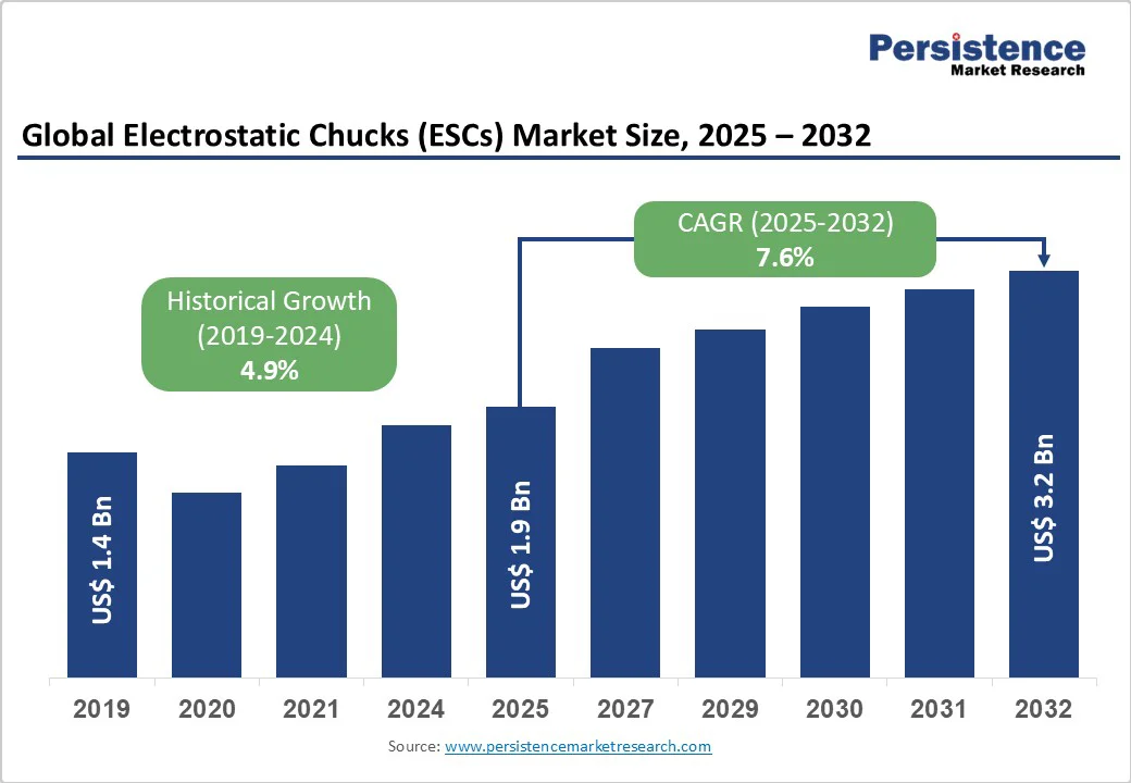
The global Electrostatic Chucks (ESCs) Market size is projected to rise from US$1.9 Bn in 2025 to US$3.2 Bn, growing at a CAGR of 7.6% during the forecast period from 2025 to 2032. Increasing demand for smaller, faster, and more efficient semiconductor and display devices is driving the adoption of ESCs in fabs and cleanroom environments. The need for higher throughput, improved yield, and effective thermal management in wafer processing is further fueling market growth. Technological advancements, such as Johnsen-Rahbek ESCs offering enhanced clamping force and uniformity, are creating new opportunities.
Key Industry Highlights:
- Leading Technology: Coulomb ESCs dominate with over 68% share in 2025, offering precise wafer handling, stable clamping under high-temperature and vacuum conditions, and compatibility with advanced semiconductor processes. Johnsen-Rahbek (JR) ESCs are the fastest-growing segment due to superior holding force and enhanced thermal conductivity for larger, high-power wafers.
- Leading Material: Ceramic lead with more than 86% share in 2025, driven by thermal stability, electrical insulation, and mechanical strength essential for advanced semiconductor fabrication. Quartz shows significant growth potential for precision wafer handling, low dielectric loss, and high flatness in advanced nodes.
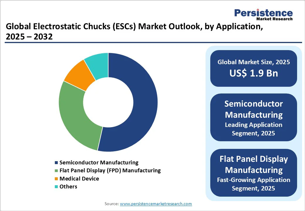
- Leading Application: Semiconductor manufacturing accounts for over 57% share in 2025, driven by precise wafer clamping, thermal uniformity, and particle-free operation for advanced nodes. Flat panel displays are a fast-growing segment due to the need for defect-free handling of delicate glass and semiconductor substrates.
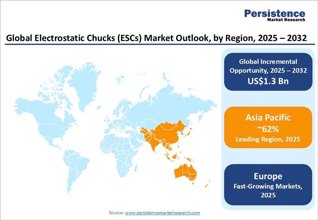
- Leading Region: Asia Pacific is the largest market with over 62% share in 2025, benefits from well-established ceramic material supply chains, precision manufacturing capabilities, & strong government support.
| Key Insights | Details |
|---|---|
|
Electrostatic Chucks (ESCs) Market Size (2025E) |
US$1.9 Bn |
|
Market Value Forecast (2032F) |
US$3.2 Bn |
|
Projected Growth (CAGR 2025 to 2032) |
7.6% |
|
Historical Market Growth (CAGR 2019 to 2024) |
4.9% |
Market Dynamics
Driver - Advancements in Photolithography and Etch Processes
The shift toward extreme ultraviolet (EUV) lithography and the proliferation of advanced etch technologies are fueling ESC market growth. ESCs facilitate precise wafer handling and thermal management, crucial for successful multi-patterning and high-aspect ratio etching. The International Roadmap for Devices and Systems (IRDS) notes that EUV adoption and high-NA tools will be the norm at leading-edge nodes by 2026-2027. Current-generation EUV and advanced etch systems utilize enhanced electrostatic chucks with superior clamping forces and thermal uniformity. As foundries pursue tighter critical-dimension (CD) control and defect reduction, demand for next-generation ESCs, particularly in ceramic and quartz formats, experiences a parallel uptick.
Semiconductor Industry Expansion and Advanced Node Processing
The expansion of semiconductor fabrication facilities and the ongoing shift toward smaller nodes are fueling demand for advanced electrostatic chucks. The global semiconductor industry's expansion to support 5G infrastructure, artificial intelligence computing, and IoT devices has created unprecedented demand for precision manufacturing equipment. Advanced semiconductor processes, particularly those involving gate-all-around architectures and sub-3nm nodes, require ESCs with enhanced thermal stability and precise wafer positioning capabilities. The industry's shift toward 300mm and emerging 450mm wafer fabrication necessitates larger, more sophisticated ESCs capable of handling increased substrate sizes while maintaining nanometer-level precision.
Restraint - Volatility in Semiconductor Equipment Capex Cycles
The ESC is heavily exposed to cyclical variations in semiconductor equipment capital expenditures. Downward swings in wafer fab utilization rates or extended inventory corrections, such as those seen during 2023-2024, result in sudden project delays and decreased order volumes for ESC suppliers. International manufacturing association SEMI reports a typical year-over-year swing of ±10-25% in equipment spending, with escalation risk from trade tensions and macroeconomic uncertainty.
Supply Chain Constraints and Raw Material Availability
Limited availability of specialized raw materials, such as high-purity ceramics, advanced dielectric materials, and precision electrode components, constrains ESC production. Supply chain disruptions affecting electronic components, sensors, and specialty materials driven by geopolitical tensions, natural disasters, or unforeseen events, further exacerbate shortages. The regional concentration of advanced ceramic manufacturing increases vulnerability to disruptions and transportation delays. Raw material price volatility directly impacts manufacturing costs, influencing pricing strategies and market competitiveness. Customized ESC configurations required for different semiconductor processes create engineering complexity and extend development timelines.
Opportunity - Advanced Packaging and Integration Technologies
The semiconductor industry's shift toward advanced packaging techniques, including 3D stacking, system-in-package (SiP), and chiplet architectures, creates new applications for precision ESC systems. These advanced packaging processes require sophisticated wafer handling capabilities during assembly and testing phases. The integration of artificial intelligence and machine learning capabilities into ESC systems for predictive maintenance and process optimization represents significant value-addition opportunities. Development of multi-zone ESCs with embedded MEMS sensors and feedback control systems enables dynamic process optimization and improved manufacturing yields.
Sustainable Manufacturing and Energy Efficiency Initiatives
Policy shifts and customer demand for lower energy consumption in cleanroom operations are driving interest in ESCs optimized for reduced power usage and longer lifecycle durability. Collaboration on sustainable equipment standards and circular economy initiatives (e.g., SEMI S23, EPEAT) offers competitive advantages for eco-friendly ESC suppliers. Innovations such as self-cleaning ESCs with plasma-repellent coatings minimize contamination and extend component lifespan, while energy-efficient designs support manufacturers’ environmental objectives.
Category-wise Analysis
By Technology, Coulomb ESCs Leading Demand Through High-Precision Wafer Handling
Coulomb ESCs are expected to account for more than 68% share in 2025, due to their strong suitability for processes requiring stable wafer clamping under high-temperature and vacuum conditions, such as plasma etching and CVD. They offer excellent uniformity, lower particle contamination, and compatibility with various wafer materials. The increasing demand for precise temperature control and process reliability in advanced semiconductor manufacturing further boosts their adoption. The growing demand for advanced semiconductor devices driven by 5G, artificial intelligence, and IoT applications has significantly boosted Coulomb ESC adoption across leading semiconductor fabs.
Johnsen-Rahbek (JR) ESCs are expected to grow at a significant rate due to their superior holding force, making them ideal for handling larger and heavier wafers. Their enhanced thermal conductivity addresses the need for precise temperature control during high-power applications. Increasing demand for high-density and high-performance chips in electronics, coupled with the need for reliable wafer stability during deposition and etching, is driving adoption. JR ESCs’ ability to minimize wafer slip and improve process yield aligns with the industry’s quality and efficiency requirements.
By Material, Ceramics Driving ESC Adoption Through Thermal Stability and Process Reliability
Ceramics are expected to account for over 86% share in 2025 due to their superior thermal stability, electrical insulation, and mechanical strength, which are essential for advanced semiconductor manufacturing processes. They provide precise wafer temperature control and uniform clamping during etching and deposition. The growing need for high-performance materials in EUV lithography and high-temperature plasma processes further drives ceramic ESC adoption. Their durability and contamination resistance make them ideal for maintaining wafer yield and process reliability.
Quartz-based ESCs are expected to grow significantly due to their superior thermal stability, low dielectric loss, and high flatness, which are critical for precision wafer handling in advanced semiconductor fabrication. As chip geometries shrink and process temperatures rise, manufacturers increasingly require materials that maintain uniform electrostatic force without causing wafer damage. Quartz enables higher throughput and longer operational life, meeting the semiconductor industry’s demand for reliability and efficiency. Rising adoption of high-end applications such as 3D ICs further fuels this growth.
By Application, Semiconductor Manufacturing Driving High-Performance ESC Adoption
Semiconductor manufacturing is expected to account for more than 57% share in 2025, its critical role in wafer handling during etching, deposition, and lithography processes. ESCs provide precise wafer clamping, superior thermal uniformity, and particle-free operation essential for advanced node fabrication. The growing demand for smaller, more powerful chips in electronics and AI applications drives fabs to adopt high-performance ESCs. The semiconductor fabrication industry's transition to advanced nodes and complex device architectures has increased ESC requirements for precision wafer positioning and thermal management.
Flat panel display is set to drive significant growth due to the industry’s need for precise and defect-free handling of delicate glass and semiconductor substrates. As demand for high-resolution displays in TVs, smartphones, and tablets rises, manufacturers require ESCs to ensure stable wafer gripping during deposition, etching, and inspection processes. This minimizes damage, enhances yield, and supports high-volume production, making ESCs critical for efficient FPD fabrication. The shift toward larger and thinner panels further increases reliance on advanced ESC technology.
Regional Insights
North America Electrostatic Chucks (ESCs) Market Trends
North America electrostatic chucks (ESCs) market leads, driven by a robust semiconductor ecosystem, high ESC adoption, and presence of major players like Applied Materials and Lam Research. Government initiatives such as the CHIPS and Science Act, along with investments in 5G infrastructure and advanced display technologies, are accelerating domestic ESC development and localization of ceramic components. Strong industry research collaboration and federal incentives support innovation, precise wafer handling, and contamination control at advanced nodes. Samsung’s planned $40 billion greenfield investment in Taylor, Texas, underscores the region’s strategic importance, transforming it into a hub for cutting-edge semiconductor manufacturing.
Asia Pacific Electrostatic Chucks (ESCs) Market Trends
Asia Pacific is expected to account for a share of more than 62% in 2025, driven by massive semiconductor manufacturing across China, Japan, South Korea, and Taiwan. The region’s top foundries and IDMs create substantial demand, supported by China’s National Integrated Circuit Industry Investment Fund III ($47.5B) and Huawei, which has boosted the yield of its latest AI chips to nearly 40%. Japan’s SHINKO, KYOCERA, and TOTO lead advanced ESC production, while South Korea grows rapidly through Samsung and SK Hynix investments. Taiwan’s contract manufacturing dominance, along with established ceramic material supply chains, precision manufacturing, and supportive government initiatives, positions Asia Pacific as the global hub for advanced ESC technologies, with India and ASEAN emerging as high-potential markets.
Europe Electrostatic Chucks (ESCs) Market Trends
Europe’s electrostatic chucks (ESCs) market is driven by high-value manufacturing hubs in Germany, the U.K., France, and Spain, with Germany leading due to its robust semiconductor capital equipment sector and EU-backed European Chips Act. Harmonized environmental and worker safety regulations accelerate cross-border supply, while R&D collaborations with institutes like Fraunhofer and IMEC enhance technology transfer and innovation. Green transition policies and EU funding drive energy-efficient, low-emission ESC production, with wafer-level innovations targeting automotive-grade and power electronics applications. In the U.K., automotive manufacturing alone contributes £93?billion in turnover and £22?billion in value added, investing around £4?billion annually in R&D, fueled by rising electric vehicle adoption and demand for power semiconductors.
Competitive Landscape
The electrostatic chucks (ESCs) market is moderately fragmented, with competition driven by a mix of global and regional manufacturers focusing on innovation and performance reliability. Leading players emphasize the development of advanced materials, improved thermal management, and enhanced wafer-holding stability to meet the demands of semiconductor fabrication. Companies also differentiate through customized ESC designs tailored for specific deposition and etching processes, ensuring higher yield and productivity.
Key Industry Developments:
- In September 2023, the semiconductor industry adopted scanning acoustic microscopy (SAM) as an advanced inspection tool to enhance the reliability of electrostatic chucks used in wafer fabrication. SAM enables non-destructive, high-resolution detection of defects such as cracks, pores, and dielectric thickness variations within sintered ESC structures. Companies like OKOS are offering specialized SAM systems for precise multi-layer inspection, ensuring superior ESC quality and performance in semiconductor manufacturing.
Companies Covered in Electrostatic Chucks (ESCs) Market
- SHINKO ELECTRIC INDUSTRIES CO. LTD.
- TOTO LTD.
- NGK INSULATORS, LTD.
- KYOCERA Corporation
- NTK CERATEC CO., LTD.
- Entegris, Inc.
- CREATIVE TECHNOLOGY CO.
- TOMOEGAWA CO., LTD.
- MiCo Co., Ltd.
- BOBOO Hightech Co., Ltd.
- Others
Frequently Asked Questions
The global electrostatic chucks (ESCs) market is projected to be valued at US$1.9 Bn in 2025.
The need for precise, uniform wafer handling and high thermal stability is a key driver.
The electrostatic chucks (ESCs)market is poised to witness a CAGR of 7.6% from 2025 to 2032.
Increasing demand for smaller and more powerful chips and the expansion of fab facilities create strong growth opportunities.
SHINKO ELECTRIC INDUSTRIES CO. LTD., TOTO LTD., NGK INSULATORS, LTD., KYOCERA Corporation, NTK CERATEC CO., LTD., Entegris, Inc., are among the leading key players.


