


- Smart Packaging
- Panel Level Packaging Market
Panel Level Packaging Market Size, Share, and Growth Forecast, 2026 - 2033
Panel Level Packaging Market by Technology Type (Fan-Out Panel-Level Packaging (FO-PLP), Panel-Level System-In-Package (PL-SIP), Others), Carrier Type (Rigid Carrier, Organic Substrate Carrier, Others), End-user, and Regional Analysis for 2026 - 2033
Panel Level Packaging Market Size and Trends Analysis
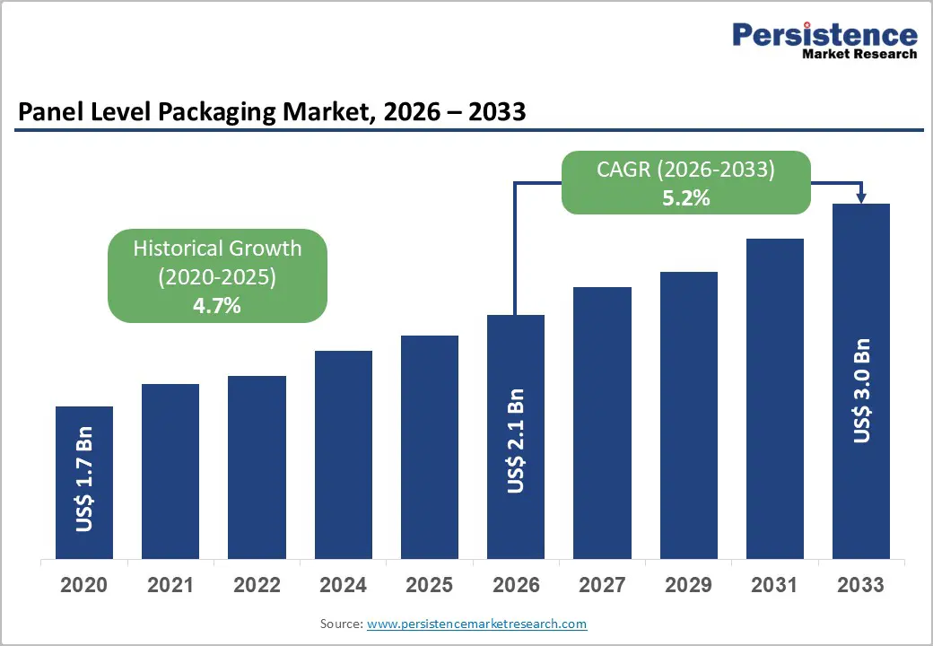
The global panel level packaging market size is likely to be valued at US$2.1 billion in 2026 and is expected to reach US$3.0 billion by 2033, growing at a CAGR of 5.2% between 2026 and 2033, driven by the structural shift from wafer-based to panel-based processing, which delivers higher area utilization, improved throughput, and lower per-unit packaging costs.
Accelerating demand from AI/HPC workloads, 5G infrastructure, and high-volume consumer electronics, combined with large capital investments by outsourced semiconductor assembly and test providers (OSATs) and foundries, is pushing PLP from pilot environments into early commercial deployment. Government incentives, national industrial programs, and the continued move toward system-level integration and chiplet architectures position PLP as a strategic enabler within advanced semiconductor packaging value chains.
Key Industry Highlights
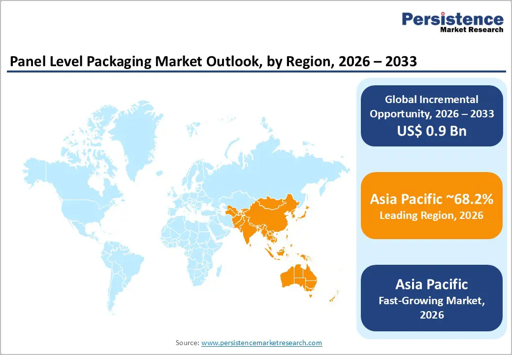
- Leading Region: Asia Pacific is projected to hold 68.2% of market share, supported by a strong OSAT ecosystem, integrated semiconductor supply chains, and proximity to high-volume consumer electronics manufacturing hubs in China, Taiwan, South Korea, and Japan.
- Fastest-Growing Region: Asia Pacific, driven by aggressive capacity expansion, rapid adoption of PLP for AI/HPC and advanced consumer electronics, and sustained government-backed manufacturing incentives.
- Investment Plans: Large-scale, long-term capital investments focused on panel-level pilot-to-commercial transitions, greenfield advanced packaging facilities, and material/tooling development. Investments are concentrated in Asia Pacific for volume scaling and in North America and Europe for high-value AI, HPC, and automotive-oriented PLP capacity.
- Dominant Technology: Fan-Out Panel-Level Packaging (FO-PLP) is estimated to account for approximately 47.6% market share, due to its commercial maturity, cost efficiency, and strong adoption in high-volume consumer and mobile electronics applications.
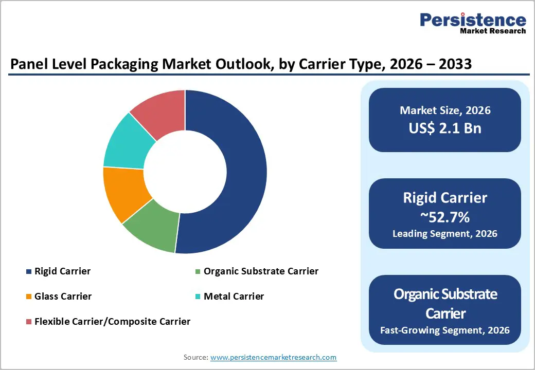
- Leading Carrier Type: Rigid carriers, holding an estimated 52.7% market share, supported by established process maturity, mechanical stability, and compatibility with existing assembly infrastructure, making them the preferred choice for early PLP commercialization.
| Key Insights | Details |
|---|---|
| Panel Level Packaging Market Size (2026E) | US$2.1 Bn |
| Market Value Forecast (2033F) | US$3.0 Bn |
| Projected Growth (CAGR 2026 to 2033) | 5.2% |
| Historical Market Growth (CAGR 2020 to 2025) | 4.7% |
Market Factors - Growth, Barriers, and Opportunity Analysis
Growth Analysis - Cost and Throughput Advantages of Panel-Based Processing
Panel-level processing offers clear economic advantages over traditional wafer-level approaches by replacing circular wafers with rectangular panels, significantly improving usable surface area and reducing edge losses. This higher area utilization allows more packages per processing cycle and enables larger reticle footprints, lowering cost per input/output and per square millimeter. For high-volume products, particularly consumer and AI-oriented packages, these efficiencies translate directly into reduced per-unit packaging cost. As chip designs increasingly adopt multi-die and chiplet architectures, panel processing reduces handling steps and supports higher automation levels, strengthening its commercial attractiveness.
Demand Pull from AI, HPC, 5G, and Consumer Electronics
Rapid growth in artificial intelligence, high-performance computing, and 5G infrastructure is increasing demand for advanced packages with high I/O density, high bandwidth, and large form factors. PLP supports these requirements by enabling dense redistribution layers and large multi-die assemblies on a single panel. At the same time, consumer electronics manufacturers continue to demand thinner, lighter, and more compact packages at aggressive cost targets. This dual demand from premium computing and mass-market consumer devices creates a stable, diversified demand base that supports sustained investment in PLP capacity.
Policy Support and Capacity Investments
Public incentives and national semiconductor strategies have materially reduced the financial risk associated with advanced packaging investments. Government funding, grants, and tax incentives aimed at strengthening domestic semiconductor supply chains are accelerating the development of panel-level pilot lines and early commercial facilities. These initiatives shorten the time required to move PLP technologies from laboratory validation to production-scale deployment and encourage closer collaboration between equipment suppliers, material vendors, and packaging providers. Policy support has become a meaningful catalyst for scaling PLP beyond experimental use cases.
Barrier Analysis - Tooling and Process Maturity Limitations
Panel-level packaging requires specialized lithography, handling, and redistribution layer tooling that is less mature than established wafer-level equipment. Yield learning curves, process variability at large panel sizes, and the need for new automation solutions increase technical risk and extend time to volume production. As a result, PLP adoption is proceeding incrementally, beginning with fan-out and selected system-in-package designs while high-end interposer applications continue to rely on proven wafer-based approaches. Early yield shortfalls and extended qualification timelines represent tangible revenue-timing risks for adopters.
Supply Chain and Material Constraints
The availability of large, high-quality carrier materials, including organic panels and glass substrates, remains constrained. Producing dimensionally stable panels with fine-pitch interconnect capability requires new supplier capacity and lengthy qualification processes. Organic substrate lead times and high-density routing capabilities can also limit near-term scalability. These constraints increase capital requirements and can compress margins during early production phases, while delays in material qualification may slow time-to-market for new PLP offerings.
Opportunity Analysis - Automotive and Electric Vehicle Electronics
Automotive electronics represent a high-value opportunity for PLP due to stringent reliability, thermal performance, and integration requirements. If PLP captures a conservative 10-15% share of automotive-oriented advanced packaging demand by 2033, this would equate to approximately US$0.3-0.45 billion of the projected US$3.0 billion PLP market. Long vehicle program lifecycles and higher average selling prices support stable revenue streams and justify the upfront cost of automotive-grade qualification. System consolidation and weight reduction trends further reinforce PLP adoption in electric and autonomous vehicles.
High-End Glass-Based PLP for AI and HPC
Glass-based panel packaging enables extremely large, high-performance packages suitable for advanced AI accelerators combining multiple logic dies and high-bandwidth memory stacks. While initially a niche segment, glass-based PLP commands premium pricing due to its dimensional stability and fine-line routing capability. Capturing even 5-8% of the total PLP market by 2033 would generate a meaningful high-margin revenue pool. Early adopters with proprietary glass processing expertise and strong customer relationships are positioned to secure long-term strategic roles in next-generation computing platforms.
Category-wise Analysis
Technology Insights
FO-PLP is anticipated to account for the largest share of approximately 47.6% in 2026, particularly in high-volume consumer and mobile electronics. By eliminating the need for conventional substrates, FO-PLP enables thinner, lighter packages while improving electrical performance and reducing material costs. Its process flow extends wafer-level fan-out techniques onto panels, maintaining familiar tooling and workflows, which accelerates adoption. FO-PLP is widely used in smartphones, tablets, AR/VR modules, and IoT devices, where compactness and cost efficiency are critical. Many OSATs have targeted FO-PLP as their first panel deployment, leveraging the mature process window to achieve high throughput at lower per-unit cost.
PL-SiP is likely to be the fastest-growing technology segment, as demand for heterogeneous integration accelerates. PL-SiP combines logic, memory, RF, and power components into a single panel-level module, enabling reduced system footprint, improved thermal management, and enhanced electromagnetic compatibility. Key applications include 5G base stations, AI accelerator modules, automotive infotainment systems, and sensor fusion packages, where multi-die integration is critical. Growth is further driven by the adoption of chiplet-based architectures, which allow multiple smaller dies to form a high-performance package, and by enterprise and automotive customers seeking system-level consolidation for reliability and performance.
Carrier Type Insights
Rigid carriers are expected to be the largest segment, with an anticipated market share of 52.7% in 2026, owing to their compatibility with existing assembly lines and established mechanical stability. Rigid panels (organic or composite cores) enable pick-and-place, molding, and testing operations with minimal process adaptation, reducing qualification risk and enabling faster commercialization. They are commonly used in consumer electronics, industrial IoT modules, and lower-to-mid-tier automotive applications, where high-volume throughput and thermal robustness are critical. Many early PLP pilot lines favor rigid carriers due to their reliability and process maturity, making them the go-to choice for initial commercial deployments.
Organic substrate carriers are likely to be the fastest-growing segment, as these carriers provide high-density routing and multilayer redistribution, supporting complex interconnect requirements for high-performance applications. Organic substrates are increasingly adopted for AI/HPC modules, high-end smartphones, and advanced automotive electronics, where dense I/Os and multi-layer connections are necessary. While glass carriers remain a niche for ultra-high-end packages, organic substrates offer a cost-effective path for scaling high-density PLP, with continued innovation in panel-scale handling and substrate design further accelerating adoption.
Regional Insights
North America Panel Level Packaging Market Trends - AI-Driven Demand and CHIPS-Backed Advanced Packaging Expansion
North America plays a strategic role in the global PLP market, particularly as a hub for AI, high-performance computing (HPC), and advanced semiconductor design. While the region does not lead in production volumes, it represents a substantial share of high-value demand driven by hyperscalers, cloud service providers, and AI accelerator developers. Public incentives, such as the CHIPS Act, are reducing investment risk and accelerating the establishment of advanced packaging lines. For example, Amkor Technology is building a greenfield advanced packaging campus in Peoria, Arizona, supported by CHIPS funding, which will serve hyperscaler clients and strengthen domestic PLP capabilities. Similarly, TSMC’s U.S. expansion includes integrated packaging operations that enhance local supply for AI and HPC applications.
Key growth drivers include the escalating demand for multi-die AI packages, government-backed capacity expansion, and tighter integration between design, fabrication, and packaging operations. The regulatory framework emphasizes supply-chain resilience and security, raising compliance requirements but creating higher barriers to entry for new entrants. Investment activity focuses on greenfield facilities, co-investment with hyperscalers, and collaborative ecosystem partnerships that shorten qualification timelines and secure long-term supply commitments. These initiatives collectively strengthen North America’s position in the high-value segment of the PLP market, even as Asia Pacific leads in volume.
Europe Panel Level Packaging Market Trends-Automotive-Focused PLP and High-Reliability Industrial Packaging
Europe’s PLP market remains smaller in volume but is strategically oriented toward automotive, industrial, and specialized electronics applications. Demand emphasizes reliability, long product lifecycles, and compliance with stringent safety and environmental standards. Selective public funding, such as grants for pilot lines and collaborative research projects, supports the development of domestic packaging capabilities rather than mass-market production. For instance, STMicroelectronics has established a US$60 million PLP pilot line in Tours, France, targeting automotive and industrial applications, while partnerships with regional Tier-1 automotive suppliers strengthen system-level integration capabilities.
Primary growth drivers include automotive electrification, industrial automation, and semiconductor sovereignty initiatives, which encourage investment in specialized PLP technologies. Regulatory requirements, though increasing upfront qualification costs, enhance supplier stickiness and long-term customer relationships. Investment trends favor targeted pilot deployments, partnerships between OEMs and OSATs, and R&D collaborations with universities and research institutions, ensuring that European PLP players remain competitive in high-reliability segments. This strategic approach enables Europe to secure automotive and industrial packages with stable, long-term contracts.
Asia Pacific Panel Level Packaging Market Trends - High-Volume PLP Manufacturing and Advanced Packaging Scale Leadership
Asia Pacific is expected to dominate the PLP market with an estimated 68.2% share, driven by its robust OSAT ecosystem, integrated supply chains, and proximity to major consumer electronics manufacturers. Taiwan, South Korea, China, and Japan lead production, supplying both high-volume and high-end PLP packages. ASE Technology and JCET in Taiwan, along with Samsung Electronics in South Korea, are expanding panel-level packaging capacity to meet increasing demand for smartphones, wearables, and AI/HPC modules. In Japan, companies such as Rapidus are developing glass panel interposers for high-performance computing applications, highlighting the region’s move toward advanced PLP materials.
Growth is fueled by large-scale consumer electronics production, rapid adoption of advanced packaging for AI and HPC applications, and aggressive investment in capacity expansion. National industrial policies and private capital investment accelerate the development of panel-level tooling, organic and glass carriers, and material innovation. Asia Pacific’s dominance in both volume and high-end segments is reinforced by its ability to quickly scale production, secure long-term customer contracts, and maintain a deep, skilled workforce capable of implementing complex panel-level packaging solutions. These factors collectively ensure the region’s leadership in global PLP deployment and innovation.
Competitive Landscape
The global panel level packaging market is transitioning from fragmented pilot activity toward an early-stage oligopolistic structure. A small group of well-capitalized OSATs, foundries, and integrated device manufacturers is consolidating early commercial capacity, while smaller players focus on niche technologies and materials. High capital intensity and qualification requirements favor established incumbents, though regional policy support continues to encourage competitive entry.
Market leaders prioritize scale, technology differentiation, and customer lock-in through long-term supply agreements. Emerging strategies include customer co-investment models, regional localization of packaging capacity, and vertical integration across design, fabrication, and assembly.
Key Industry Developments
- In November 2025, SCHMID Group secured major equipment orders for Panel Level Packaging and modified-Semi-Additive Process production systems from customers in Southeast Asia and China, reflecting rising PLP and mSAP demand.
- In October 2025, Amkor Technology announced the groundbreaking of its new semiconductor advanced packaging and test campus in Arizona with an expanded investment of US$7 billion, designed to support high-volume PLP and advanced packaging services and strengthen U.S. capabilities for AI and high-performance computing demand.
Companies Covered in Panel Level Packaging Market
- ASE Technology Holding
- Amkor Technology
- Taiwan Semiconductor Manufacturing Company
- Samsung Electronics
- Intel Corporation
- JCET Group
- STMicroelectronics
- Tongfu Microelectronics
- Siliconware Precision Industries
Frequently Asked Questions
The global panel level packaging market size is valued at US$2.1 billion in 2026.
By 2033, the panel level packaging market is expected to reach US$3.0 billion.
Key trends include the shift from wafer-level to panel-level processing to improve area utilization and reduce per-unit cost, rising adoption of fan-out PLP in high-volume consumer devices, growing demand for heterogeneous integration and chiplet-based architectures, increasing investments in glass and organic panel carriers, and strong policy-driven capacity expansion in advanced packaging.
Fan-Out Panel-Level Packaging (FO-PLP) is the leading segment, accounting for approximately 47.6% of market share, driven by its cost efficiency, commercial maturity, and suitability for high-volume consumer and mobile electronics.
The PLP market is projected to grow at a CAGR of 5.2% between 2026 and 2033.
Major players include ASE Technology Holding Co., Ltd., Amkor Technology, Inc., TSMC (Taiwan Semiconductor Manufacturing Company), Samsung Electronics, and JCET Group.


