


- Smart Packaging
- 3D IC and 2.5D IC Packaging Market
3D IC and 2.5D IC Packaging Market Size, Share, and Growth Forecast, 2026 - 2033
3D IC and 2.5D IC Packaging Market by Packaging Technology (3D IC Packaging, 2.5D IC Packaging, Others), Application (High Performance Computing (HPC), Consumer Electronics, Others), End-use Industry, and Regional Analysis for 2026 - 2033
3D IC and 2.5D IC Packaging Market Size and Trends Analysis
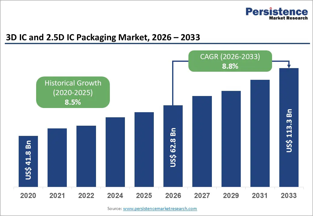
The global 3D IC and 2.5D IC packaging market size is likely to be valued at US$62.8 billion in 2026 and is expected to reach US$113.3 billion by 2033, growing at a CAGR of 8.8% between 2026 and 2033, driven by rising requirements for high-bandwidth, energy-efficient semiconductor architectures supporting AI and high-performance computing workloads.
The transition from monolithic scaling toward chiplet-based designs, combined with increasing adoption of hybrid bonding and through-silicon via (TSV) technologies, is reshaping semiconductor integration strategies. Hyperscale data center expansion, HBM memory deployment for accelerators, and capacity additions across Asia Pacific and North America remain the primary commercial growth levers, supported by sustained investments in advanced packaging fabs and OSAT capability upgrades.
Key Industry Highlights
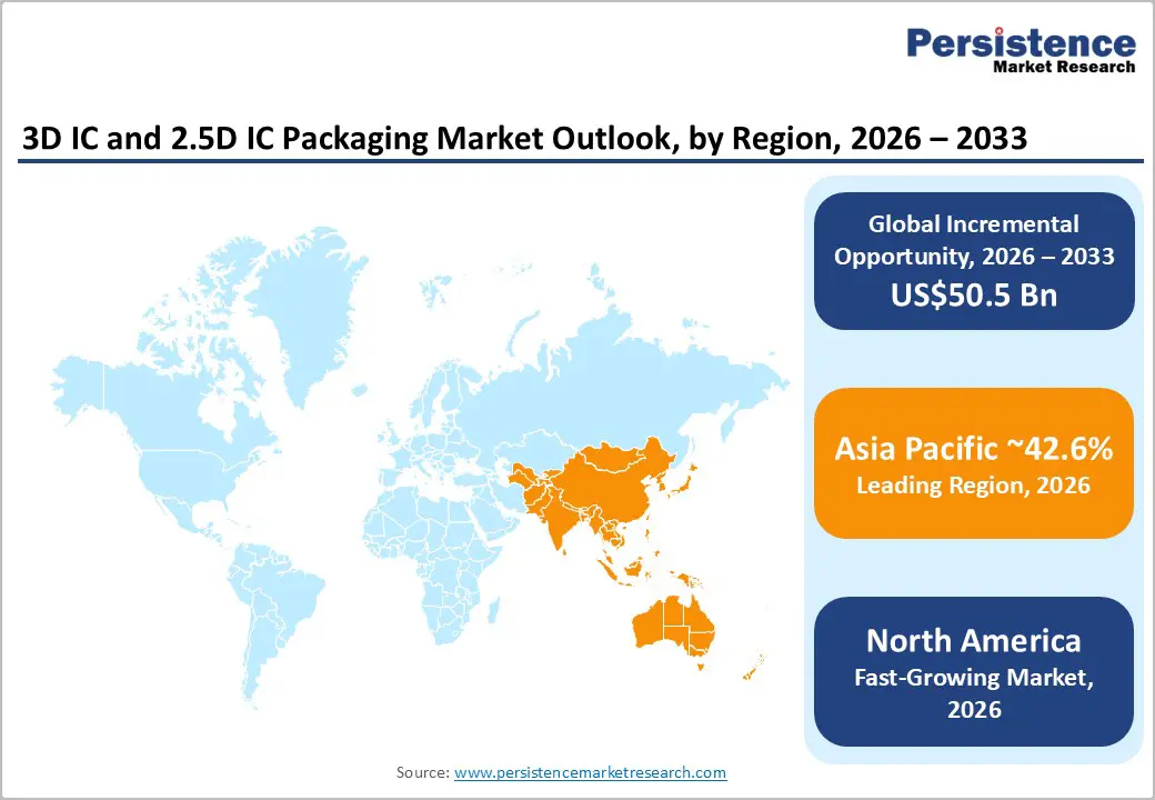
- Leading Region: Asia Pacific, is projected to account for approximately 42.6% of market share in 2026, supported by its integrated ecosystem of advanced foundries, OSATs, substrate suppliers, and high-volume electronics manufacturing, with Taiwan, South Korea, and Japan anchoring leadership in 3D and 2.5D packaging capacity.
- Fastest-growing Region: North America, to exhibit the highest value growth rate during the forecast period, driven by rising adoption of advanced packaging in AI accelerators, hyperscale data centers, and defense applications, alongside government-backed investments under the U.S. CHIPS and Science Act.
- Investment Plans: Large-scale capital investments exceeding multiple billions of U.S. dollars globally, focused on hybrid bonding, TSV scaling, and interposer capacity expansion, led by foundries and OSATs in Asia Pacific and reinforced by policy-driven funding in the U.S. and Europe to strengthen domestic advanced packaging capabilities.
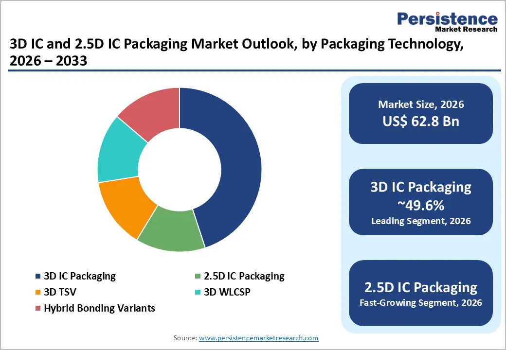
- Dominant Packaging Technology: 3D IC Packaging, anticipated to hold over 49.6% revenue share, driven by widespread deployment in high-bandwidth memory (HBM) stacks, AI accelerators, and high-performance computing platforms requiring ultra-high interconnect density and power efficiency.
- Leading Application: High-Performance Computing (HPC) is estimated to account for over 36.7% of revenue share, supported by sustained growth in AI training, inference workloads, and data-center-scale compute infrastructure requiring advanced 2.5D and 3D integration.
| Key Insights | Details |
|---|---|
| 3D IC and 2.5D IC Packaging Market Size (2026E) | US$62.8 Bn |
| Market Value Forecast (2033F) | US$113.3 Bn |
| Projected Growth (CAGR 2026 to 2033) | 8.8% |
| Historical Market Growth (CAGR 2020 to 2025) | 8.5% |
Market Factors - Growth, Barriers, and Opportunity Analysis
Growth Analysis - AI/HPC Demand and HBM-Memory-Led Bandwidth Requirements
The rapid scaling of artificial intelligence models and high-performance computing workloads has generated unprecedented demand for semiconductor packages capable of delivering extremely high memory bandwidth with minimal latency. High-Bandwidth Memory (HBM) integrated through 2.5D interposers and 3D-stacked die architectures enables terabytes-per-second data transfer while lowering power consumption per computation.
These capabilities are essential for modern accelerators used in data centers and advanced analytics. As compute intensity rises faster than traditional process scaling benefits, system designers increasingly rely on advanced packaging rather than transistor shrinkage alone. This shift has driven large capital commitments toward TSV formation, hybrid bonding equipment, and interposer manufacturing capacity, reinforcing advanced packaging as a strategic enabler of next-generation compute performance.
Chiplet Economics and Heterogeneous Integration
As mask costs and design complexity escalate at advanced process nodes, chiplet-based architectures assembled through 2.5D and 3D packaging provide a more economically sustainable path to performance scaling. Chiplets allow system designers to combine logic, memory, analog, and specialized accelerators manufactured on different nodes within a single package, improving yield and reducing development risk.
This approach accelerates time-to-market through IP reuse while enabling rapid architectural iteration. Standardized die-to-die interfaces and collaborative ecosystems across foundries, OSATs, and integrated device manufacturers are reinforcing this transition. As heterogeneous integration becomes central to product roadmaps, demand for high-density interposers, advanced RDL processes, and precision bonding services continues to rise.
Regional Capacity Buildouts and Supply-Chain Diversification
Governments and large semiconductor customers are increasingly prioritizing supply-chain resilience through localized advanced packaging capacity. Public incentives, national semiconductor strategies, and long-term customer commitments are accelerating investments in new packaging facilities, cleanroom infrastructure, and skilled workforce development. North America and Europe are expanding domestic capabilities to support strategic AI and defense requirements, while Asia Pacific continues to leverage its mature OSAT ecosystem and scale efficiencies. These coordinated capacity expansions are improving near-to-mid-term supply availability for 2.5D and 3D packaging technologies and reducing systemic risk associated with geographic concentration.
Barrier Analysis -High Capital Intensity and Long Ramp-Up Cycles
Advanced 2.5D and 3D packaging requires substantial capital investment in specialized equipment, including hybrid bonders, TSV tools, high-precision alignment systems, and interposer fabrication lines. Cleanroom specifications often exceed those of conventional packaging facilities, significantly increasing upfront costs. Greenfield projects can involve multi-hundred-million to multi-billion-dollar investments, with ramp-up periods extending three to five years. These long timelines heighten utilization risk and expose investors to demand-cycle volatility and technology shifts, particularly if market adoption deviates from initial projections.
Thermal, Reliability, and Design Complexity
Dense vertical integration introduces significant thermal management and mechanical reliability challenges. 3D stacking intensifies heat dissipation requirements and increases susceptibility to warpage, interconnect cracking, and bonding misalignment, which can reduce yield and increase cost per functional device. Qualification cycles for automotive, aerospace, and other safety-critical applications are considerably longer than for consumer electronics, further delaying commercialization. Until standardized design-for-manufacturing and test methodologies mature, these technical complexities will continue to constrain broader adoption in high-reliability end markets.
Opportunity Analysis - Standardization and Chiplet Ecosystem Services
The emergence of standardized die-to-die interconnects and open chiplet ecosystems creates a significant opportunity for advanced packaging providers to move beyond assembly-only roles. Turnkey integration services encompassing validation, co-design, supply-chain coordination, and IP interoperability enable faster customer adoption and higher value capture. Certified chiplet marketplaces and pre-qualified package architectures reduce integration risk for system designers, particularly in AI and telecommunications. Providers that establish robust, repeatable chiplet-to-package workflows are positioned to secure long-term, cross-industry engagements and premium service margins.
Automotive Electronics and Edge Computing
The evolution of automotive electronics toward centralized domain controllers and sensor-rich architectures is driving demand for compact, high-reliability semiconductor packages. 3D and 2.5D packaging enables tight integration of compute, memory, and sensing elements within constrained automotive form factors, supporting advanced driver assistance and electric vehicle platforms. Similarly, edge computing applications require energy-efficient, ruggedized modules capable of real-time inference. Suppliers that achieve automotive-grade qualification and offer advanced thermal management solutions can capture long-duration design wins with strong pricing power and predictable revenue streams.
Category-wise Analysis
Packaging Technology Insights
3D IC packaging is expected to dominate, accounting for over 49.6% of revenue share in 2026, driven by its critical role in enabling high-density, high-bandwidth semiconductor architectures. TSV-based stacking, face-to-face hybrid bonding, and wafer-level stacking are widely deployed in HBM memory stacks, AI accelerators, and high-end CPUs and GPUs used in hyperscale data centers. The technology’s ability to minimize interconnect length, reduce signal latency, and maximize bandwidth density has made it indispensable for AI model training, real-time inference, and exascale computing platforms. Significant intellectual property investments, long-term supply agreements, and co-development partnerships between chip designers and packaging providers reinforce the leadership position of 3D IC packaging, particularly in applications where performance per watt and thermal efficiency are decisive competitive factors.
2.5D IC packaging is projected to be the fastest-growing packaging technology segment due to its optimal balance between performance enhancement, manufacturability, and cost efficiency. Interposer-based architectures enable high-density integration of logic and memory at scale while offering higher yields, improved thermal characteristics, and lower process risk compared with full 3D stacking. This approach is increasingly adopted in graphics processors, AI inference chips, high-speed networking ASICs, and advanced SoCs used in data centers and premium consumer electronics. As organic and silicon interposer technologies mature and unit costs decline, 2.5D solutions are gaining traction among chiplet-based designs, serving as a scalable and lower-risk pathway toward deeper heterogeneous and 3D integration.
Application Insights
High-performance computing is projected to be the largest application segment, holding over 36.7% of the revenue share, supported by sustained demand for AI training, generative AI workloads, scientific simulations, and large-scale data analytics. HPC systems require dense memory integration, massive I/O bandwidth, and ultra-low-latency interconnects, which are most effectively delivered through 3D-stacked memory and 2.5D interposer-based architectures. Advanced packaging is central to enabling HBM-enabled GPUs, AI accelerators, and custom compute platforms deployed in hyperscale and enterprise data centers. Long product lifecycles, high average selling prices, and performance-critical requirements support continuous investment in advanced packaging services, with co-design, reliability testing, and validation capabilities emerging as key competitive differentiators.
Consumer electronics is likely to be the fastest-growing application segments as smartphones, wearables, AR/VR devices, and premium personal computing platforms increasingly integrate on-device AI, advanced imaging, and high-performance graphics capabilities. Advanced packaging enables higher levels of functionality within thinner, lighter, and thermally constrained form factors, while improving power efficiency and signal integrity. Technologies such as fan-out wafer-level packaging, 2.5D interposers, and compact multi-die integration are being adopted to support AI-enabled processors and memory subsystems in flagship consumer devices. As manufacturing volumes scale and packaging costs gradually decline, adoption is expected to accelerate further, positioning consumer electronics as a key volume-driven growth engine over the forecast period.
Regional Insights
North America 3D IC and 2.5D IC Packaging Market Trends - AI Accelerators, Defense Programs, and Domestic Advanced Packaging
North America is estimated to be the fastest-growing region, supported by sustained demand from AI system developers, hyperscale cloud service providers, and defense-focused semiconductor programs. The region commands higher average selling prices due to its concentration on performance-critical and mission-assured applications, particularly AI accelerators, advanced GPUs, and high-bandwidth memory integration. Major U.S.-based fabless leaders such as NVIDIA, AMD, Intel, and Broadcom rely extensively on advanced 2.5D and 3D packaging for next-generation compute platforms, reinforcing domestic demand for cutting-edge packaging services.
Government-led initiatives are materially influencing market momentum. The U.S. CHIPS and Science Act has allocated funding to strengthen advanced packaging and heterogeneous integration, with Intel expanding its advanced packaging roadmap under its Foundry Services division and emphasizing EMIB and Foveros technologies. In parallel, OSAT and equipment suppliers are increasing U.S. footprints to improve supply-chain resilience. Defense and aerospace demand, driven by agencies such as the U.S. Department of Defense, further supports the adoption of high-reliability 3D packaging for secure and long-lifecycle systems, anchoring long-term growth.
Europe 3D IC and 2.5D IC Packaging Market Trends - Automotive-Grade Reliability and Regulation-Led Integration
Europe’s 3D and 2.5D IC packaging market is shaped by stringent regulatory standards, strong automotive electronics demand, and an emphasis on reliability-certified semiconductor solutions. While the region represents a smaller share of global volume compared with Asia Pacific, it benefits from high-value, application-specific niches in automotive ADAS, industrial automation, and telecommunications infrastructure. Countries such as Germany, France, and the U.K. lead demand, supported by strong automotive OEM ecosystems and industrial electronics manufacturers.
Policy alignment plays a central role. The European Chips Act prioritizes advanced packaging and heterogeneous integration as strategic capabilities, encouraging cross-border collaboration among foundries, OSATs, and research institutions. Organizations such as imec (Belgium) are instrumental in advancing hybrid bonding and 3D integration research. European semiconductor leaders, including Infineon Technologies, STMicroelectronics, and NXP Semiconductors increasingly leverage advanced packaging to integrate logic, power, and memory in compact, automotive-qualified modules. These dynamics support steady, regulation-aligned adoption rather than volume-driven expansion.
Asia Pacific 3D IC and 2.5D IC Packaging Market Trends - Foundry-OSAT Scale and High-Volume HBM Enablement
Asia Pacific is expected to be the leading regional market, accounting for approximately 42.6% of global revenue, underpinned by its deeply integrated semiconductor manufacturing ecosystem. The region hosts the world’s most advanced foundries, OSAT providers, substrate suppliers, and consumer electronics manufacturers, creating unmatched scale and execution efficiency. Taiwan remains central to market leadership, with TSMC’s large-scale deployment of CoWoS and SoIC technologies enabling advanced AI processors and HBM integration for global customers.
South Korea and Japan further reinforce regional dominance. Samsung Electronics and SK hynix drive demand for 3D TSV and hybrid bonding through high-volume HBM production, while Japanese firms such as Ibiden and Shinko Electric Industries play a critical role in advanced substrate supply. China and Southeast Asia continue to expand OSAT capacity and interposer manufacturing, supported by government-backed semiconductor localization programs. High-volume consumer electronics production, combined with sustained investment in 2.5D and 3D packaging infrastructure, ensures Asia Pacific’s continued leadership across both performance-driven and volume-driven market segments.
Competitive Landscape
The global 3D IC and 2.5D IC packaging market is moderately concentrated at the platform level, where a small number of leading foundries and integrated manufacturers define core technologies. Outsourced assembly and test services remain more fragmented, with multiple providers competing on scale, process capability, and co-engineering expertise. Competitive differentiation centers on hybrid bonding proficiency, interposer supply integration, and long-term customer partnerships.
Recent strategic developments include large-scale investments in advanced packaging campuses, the introduction of next-generation multi-chiplet integration platforms, and expanded deployment of hybrid bonding equipment. These initiatives are reducing cost per interconnect, improving yields, and accelerating the commercialization of complex heterogeneous systems, reinforcing advanced packaging as a strategic growth priority across the semiconductor industry.
Leading companies emphasize vertical integration, capacity expansion, and technology co-development to secure long-term customer relationships. Emerging strategies include service-oriented packaging models and ecosystem partnerships that support repeatable, scalable chiplet integration.
Key Industry Developments
- In June 2025, Siemens Digital Industries Software launched its Innovator3D IC suite and Calibre 3DStress tools to accelerate design, verification, and thermal analysis for complex heterogeneous 2.5D and 3D IC packages.
- In January 2025, Keysight Technologies released the Chiplet PHY Designer 2025 tool with support for advanced chiplet interconnect standards, enhancing pre-silicon validation for AI and data center applications.
Companies Covered in 3D IC and 2.5D IC Packaging Market
- TSMC
- Samsung Electronics
- Intel
- ASE Technology
- Amkor Technology
- JCET Group
- Siliconware Precision Industries (SPIL)
- Powertech Technology Inc. (PTI)
- Micron Technology
- Texas Instruments
- Broadcom
- UMC
- Samsung Electro-Mechanics
- Ibiden
- Unimicron
Frequently Asked Questions
The global 3D IC and 2.5D IC packaging market is valued at US$62.8 billion in 2026.
The 3D IC and 2.5D IC packaging market is projected to reach US$113.3 billion by 2033.
Key trends include the rising adoption of HBM-enabled AI accelerators, transition to chiplet-based architectures, increased use of hybrid bonding and TSVs, and the expanding advanced packaging capacity in Asia Pacific and North America.
3D IC packaging is the leading segment, accounting for over 49.6% market share, driven by AI, HPC, and memory stacking applications.
The 3D IC and 2.5D IC packaging market is expected to grow at a CAGR of 8.8% between 2026 and 2033.
Major players include TSMC, Samsung Electronics, Intel, ASE Technology, and Amkor Technology.


