


- Automation & Robotics
- Surface Roughness Measurement Market
Surface Roughness Measurement Market Size, Trends, Share, and Growth Forecast 2025 - 2032
Surface Roughness Measurement Market by Method (Stylus Profilometry, Optical Profilometry, Confocal Profilometry, Focus Variation, X-ray Reflectometry, Atomic Force Microscopy (AFM), Scanning Electron Microscopy (SEM), Others), Surface Type (2D, 3D), Technique (Contact, Non-contact), Industry (Automotive, Aerospace & Defence, Optics, Medical & Healthcare, Others), by Regional Analysis, 2025 - 2032
Surface Roughness Measurement Market Size and Trend Analysis
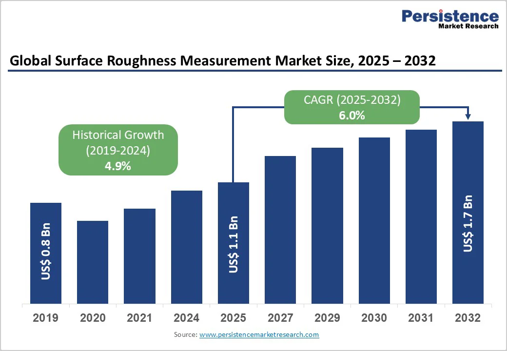
The global surface roughness measurement market size is valued at US$ 1.1 billion in 2025 and is projected to reach US$ 1.7 billion by 2032, growing at a CAGR of 6.0% between 2025 and 2032.
This consistent trajectory reflects the growing demand for precision quality control across diverse manufacturing sectors where surface characteristics directly influence component performance, durability, and regulatory compliance.
The market expansion is driven by multiple convergent factors, including increasing adoption of non-contact measurement technologies, growing semiconductor manufacturing capacity, stricter international quality standards, and the integration of surface metrology systems into automated production lines.
Key Market Highlights:
- Leading Region: North America dominates the surface roughness measurement market with approximately 29% global share in 2025, driven by sophisticated automotive, aerospace, semiconductor, and medical device manufacturing sectors.
- Fastest Growing Region: Asia Pacific expands at 7.4% CAGR through 2032, reflecting extraordinary semiconductor manufacturing capacity expansion in China, accelerating automotive production across India and Southeast Asia.
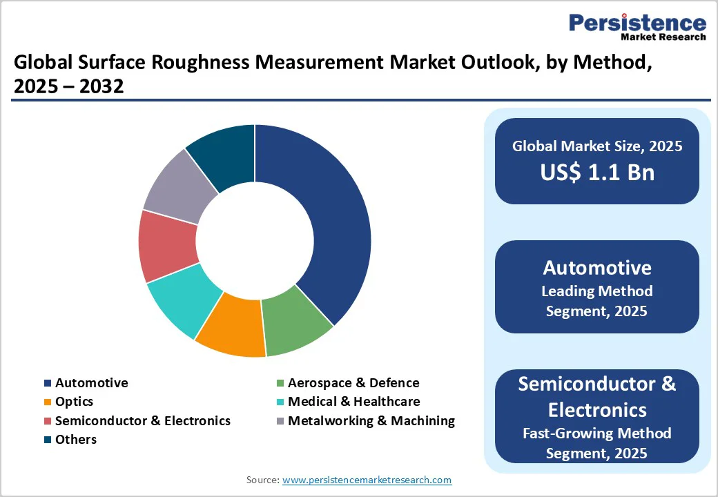
- Dominant Segment: Optical Profilometry Method commands approximately 35% market share, driven by rapid technological advancement enabling faster non-destructive surface characterization, superior measurement speed.
- Fastest Growing Segment: 3D Surface Type Measurement expands at 8.1% CAGR through 2032, reflecting industry recognition that comprehensive three-dimensional surface characterization delivers superior insight into component functionality compared to traditional 2D profile measurements.
- Key Market Opportunity: Semiconductor Advanced Packaging and Miniaturization creates exceptional growth prospects as three-dimensional integrated circuits and advanced packaging architectures demand volumetric inspection capabilities and non-destructive metrology solutions at nanoscale precision levels.
| Key Insights | Details |
|---|---|
| Surface Roughness Measurement Market Size (2025E) | US$ 1.1 Billion |
| Market Value Forecast (2032F) | US$ 1.7 Billion |
| Projected Growth CAGR (2025 - 2032) | 6.0% |
| Historical Market Growth (2019 - 2024) | 4.9% |
Market Dynamics
Drivers - Accelerating Semiconductor Manufacturing and Advanced Packaging Requirements
The semiconductor industry represents a primary growth driver for surface roughness measurement technologies, driven by the escalating complexity and miniaturization of integrated circuits and advanced packaging solutions. The global semiconductor industry is projected to grow at 8% CAGR through 2032, with particular emphasis on advanced node manufacturing requiring increasingly rigorous surface characterization.
Three-dimensional semiconductor packaging architectures demand volumetric inspection capabilities and non-destructive metrology solutions, driving adoption of advanced surface measurement technologies including atomic force microscopy (AFM), X-ray reflectometry, and confocal profilometry.
Semiconductor manufacturers require surface roughness measurements at the nanoscale level to detect minute defects, ensure proper lithography performance, and maintain yield optimization across full-wafer inspections.
The proliferation of chip-scale packaging (CSP), through-silicon vias (TSVs), and 3D integrated circuits necessitates increasingly sophisticated metrology infrastructure, creating substantial market opportunities for advanced surface measurement solution providers.
Stringent International Quality Standards and Regulatory Compliance Requirements
Global regulatory frameworks and industry-specific quality standards are compelling manufacturers across automotive, aerospace, medical device, and precision engineering sectors to adopt comprehensive surface roughness measurement protocols.
ISO 21920 and ISO 25178 standards governing surface texture measurement requirements have become mandatory compliance benchmarks across developed economies, requiring manufacturers to establish traceable measurement systems capable of delivering quantifiable surface characteristics.
MIL-STD-171 specifications for aerospace and defense applications mandate rigorous surface finish verification for critical components, driving adoption of certified measurement equipment and calibrated profilometry systems.
Medical device manufacturers operating under FDA regulations and ISO 13485 quality management systems require surface roughness specifications for implantable devices and surgical instruments, where surface texture directly impacts biocompatibility, corrosion resistance, and device longevity.
The automotive industry’s adherence to IATF 16949 quality standards and the aerospace sector’s compliance with AS9100 certifications collectively drive systematic adoption of standardized surface measurement practices, expanding market opportunities for manufacturers providing compliant metrology solutions.
Restraints - High Equipment Acquisition and Maintenance Costs Limiting Market Accessibility
Surface roughness measurement systems require substantial capital investment, with advanced optical profilometry systems, atomic force microscopes, and confocal microscopy platforms commanding equipment costs ranging from US$ 50,000 to over US$ 500,000 depending on measurement capabilities and automation features.
This significant capital requirement constrains market adoption among small and medium-sized enterprises, particularly in developing economies where budget allocations remain limited.
Equipment maintenance, regular calibration verification, software updates, and certified operator training requirements further increase total cost of ownership, potentially deterring potential customers from adopting advanced surface metrology solutions.
Additionally, specialized consumables including stylus probes, calibration standards, and optical components require ongoing replacement, incrementally increasing operational expenses and limiting customer willingness to expand measurement infrastructure across production facilities.
Technical Complexity and Specialized Expertise Requirements Creating Adoption Barriers
Surface roughness measurement systems require sophisticated understanding of measurement principles, data interpretation, and proper equipment configuration to generate meaningful results.
The technical complexity inherent in advanced metrology platforms including AFM systems, optical interferometry, and confocal profilometry necessitates specialized operator training and sustained expertise development, creating labor availability constraints in regions lacking metrology-trained professionals.
Interpretation of multidimensional surface roughness parameters, including Ra (arithmetic average roughness), Rz (maximum height), Rsk (skewness), and Rku (kurtosis) requires sophisticated understanding of surface characterization principles and ISO standards compliance.
The lack of standardized training curricula and certified metrology professionals in many developing regions impedes market expansion, particularly in Asia Pacific and Latin American markets, where manufacturing infrastructure continues developing.
Opportunity - Explosive Growth in Non-Contact Optical Measurement Technologies and Automated Inspection Systems
Non-contact optical profilometry represents one of the fastest-growing market segments, projected to expand at 9% CAGR through 2032, driven by technological advancements enabling faster, non-destructive surface characterization across diverse material types.
Advanced optical measurement techniques, including white light interferometry, confocal laser scanning microscopy, and focus variation microscopy, eliminate physical contact with measured surfaces, eliminating wear concerns and enabling measurement of delicate, soft, or reflective surfaces previously unsuitable for stylus-based contact profilometry.
The integration of 3D optical measurement systems directly into automated production lines enables real-time quality monitoring and immediate corrective action implementation, supporting the industry-wide transition toward Industry 4.0 and smart manufacturing.
The automotive and aerospace sectors’ increasing adoption of inline surface measurement systems represents a significant growth opportunity, with manufacturers progressively integrating surface metrology into production workflows rather than restricting measurements to post-production quality verification.
Emerging Medical Device and Optics Applications Driving Specialized Measurement Demand
The medical device sector represents an emerging high-growth opportunity for surface roughness measurement solutions, with implantable devices and surgical instruments requiring increasingly stringent surface finish specifications to ensure biocompatibility and performance reliability.
Advanced orthopedic implants, cardiovascular devices, and surgical instruments demand surface finishes with Ra values below 0.1 micrometers (100 nanometers), necessitating ultra-high-resolution measurement systems capable of detecting minute surface variations.
The optics industry’s expanding demand for precision optical components, including lenses, prisms, and optical coatings, drives the need for specialized surface characterization addressing sub-nanometer-scale surface properties.
Government healthcare initiatives promoting advanced medical device manufacturing, combined with rising patient population demographics in developed and emerging economies, are expected to substantially increase demand for medical device manufacturing infrastructure, proportionally increasing requirements for surface metrology and quality assurance capabilities.
Category-wise Analysis
Method Insights
The optical profilometry segment leads the surface roughness measurement market in 2025 with around 35% share, supported by strong demand for fast, accurate, and non-destructive surface characterization.
Optical profilometry methods such as white light interferometry, confocal laser scanning microscopy, and focus variation microscopy offer high-speed 3D measurement, excellent repeatability, and the ability to analyze reflective, transparent, and complex surfaces.
Automotive and aerospace manufacturers increasingly prefer optical systems to measure finished components without wear or deformation. Advanced 3D optical profilometers with sub-micron vertical resolution strengthen adoption in precision manufacturing. Continuous innovation by major metrology companies is improving automation, software intelligence, and measurement efficiency, supporting the sustained growth of the optical profilometry market.
Surface Type Insights
The 3D surface measurement segment is the fastest-growing category in the surface roughness measurement market, expected to record an 8.1% CAGR through 2032. Growth is driven by the rising need for complete 3D surface characterization that captures texture, isotropy, material volume, and surface functionality better than traditional 2D methods.
Precision machining, polishing, honing, and CMP processes increasingly rely on 3D topography assessment for process optimization and quality assurance. The semiconductor industry’s shift toward 3D ICs, advanced packaging, and wafer-level structures further accelerates adoption of volumetric measurement tools.
Meanwhile, the 2D segment holds dominant share in 2025, supported by its continued use in legacy manufacturing environments where single-profile roughness evaluation remains sufficient.
Technique Insights
Non-contact measurement dominates the surface roughness measurement market in 2025 with nearly 62% share due to its non-destructive, high-speed, and highly repeatable performance. Optical profilometry, laser scanning, X-ray reflectometry, and AFM eliminate drawbacks seen in contact stylus systems, such as tip wear, surface deformation, and difficulty measuring soft or precision-finished materials.
Automotive and aerospace industries increasingly adopt non-contact techniques for inspecting gears, bearing surfaces, and optical components where physical contact is unacceptable. Non-contact systems also support automated quality control lines and advanced manufacturing workflows.
Contact measurement retains its remaining market share due to its cost-effectiveness and relevance in metalworking processes, where stylus profilometers continue to meet functional requirements.
Industry Insights
The automotive sector leads the surface roughness measurement market with about 32% share in 2025, driven by strict quality control standards for engine parts, transmission components, bearings, and painted body panels. Surface finish plays a direct role in friction, wear, sealing performance, and vehicle durability, prompting OEMs to enforce rigorous measurement protocols across suppliers.
The shift toward electric vehicles expand demand for roughness evaluation of battery housings, electrode materials, and thermal management components. The semiconductor and electronics sector is the fastest-growing segment with a 7.8% CAGR, supported by global fab expansion and increasing integration of surface metrology into advanced chip production.
Aerospace and defense industries also maintain strong demand due to safety-critical component requirements.
Regional Insights
North America Surface Roughness Measurement Market Trends
North America maintains approximately 29% market share in 2025, positioning the region as a mature, well-established market with sophisticated measurement infrastructure and established quality control practices across automotive, aerospace, medical device, and semiconductor sectors.
The United States represents the regional growth engine, with major automotive manufacturers, semiconductor companies, and aerospace suppliers investing substantially in advanced surface metrology capabilities aligned with stringent regulatory frameworks and customer quality requirements.
The Detroit automotive cluster and Silicon Valley semiconductor ecosystem drive concentrated demand for advanced surface measurement systems, with major OEMs including General Motors, Ford Motor Company, and Intel Corporation maintaining comprehensive surface measurement protocols across production networks.
North American surface measurement practices emphasize automation integration, real-time quality monitoring, and data-driven decision-making aligned with Industry 4.0 manufacturing initiatives. The region’s aerospace sector maintains stringent surface finish requirements for commercial and defense aircraft components, driving adoption of advanced measurement technologies, including atomic force microscopy and optical profilometry systems.
Medical device manufacturers also maintain rigorous surface characterization protocols for implantable devices and surgical instruments, driving demand for specialized measurement systems capable of delivering sub-micron resolution and traceability to international standards.
Europe Surface Roughness Measurement Market Trends & Analysis
Europe represents a 27% share in 2025, characterized by manufacturing excellence, stringent regulatory frameworks, and well-established quality management practices across automotive, aerospace, and precision engineering sectors. Germany dominates European surface measurement adoption, with Daimler AG, BMW Group, Volkswagen, and Siemens AG maintaining sophisticated quality infrastructure incorporating advanced surface metrology systems.
The region’s strong manufacturing heritage, particularly concentrated in precision engineering, machine tool production, and automotive manufacturing, has established well-developed supplier ecosystems supporting surface measurement system deployment and expertise.
European manufacturers in the aerospace sector, represented by Airbus S.A.S., Rolls-Royce Holdings, and regional suppliers, maintain rigorous compliance with EASA (European Aviation Safety Agency) standards that require comprehensive surface finish verification and traceability documentation.
The United Kingdom, France, and Spain represent secondary growth markets, with established aerospace, automotive, and electronics manufacturing clusters supporting distributed surface measurement infrastructure deployment across regional supply chains.
Asia Pacific Surface Roughness Measurement Market Trends
Asia Pacific emerges as the fastest-growing regional market, projected to expand at 7.4% CAGR through 2032, reflecting extraordinary semiconductor manufacturing capacity expansion, accelerating automotive production, and increasing investment in precision engineering infrastructure across the region.
China dominates regional semiconductor manufacturing growth, with government-backed capacity expansion driving massive investments in surface metrology infrastructure to support advanced integrated circuit fabrication processes.
The region’s semiconductor industry, concentrated in Shanghai, Beijing, Shenzhen, and Chongqing, increasingly adopts advanced measurement systems to support 5G semiconductor technologies, AI processors, and advanced packaging architectures.
India’s automotive and precision manufacturing sectors represent emerging growth opportunities, with increasing foreign direct investment driving modernization of production facilities and adoption of advanced quality control systems including surface metrology.
Japan and South Korea maintain technological leadership in optical measurement systems and advanced metrology instrumentation, with companies including Keyence Corporation and Mitutoyo America Corporation headquartered in the region developing and manufacturing leading measurement platforms deployed globally.
ASEAN countries, including Vietnam, Thailand, Indonesia, and Malaysia, experience accelerating manufacturing infrastructure development, creating emerging opportunities for surface measurement system adoption as precision manufacturing expands across these developing economies.

Competitive Landscape
The surface roughness measurement market exhibits moderate consolidation characterized by the presence of specialized technology leaders commanding significant market share combined with emerging regional competitors capturing growing segments in developing economies.
ZEISS Group, Mahr Metrology, Hexagon AB, Mitutoyo Corporation, and Keyence Corporation maintain dominant competitive positions through technological sophistication, comprehensive product portfolios spanning multiple measurement methods, and extensive distribution networks reaching automotive, aerospace, semiconductor, and medical device manufacturers.
Emerging manufacturers such as Faro Technologies, Nikon Instruments, and ACCRETECH (Europe) GmbH pursue differentiated strategies emphasizing portable measurement systems, specialized applications, and cost-effective solutions for price-sensitive market segments.
Strategic partnerships between measurement equipment manufacturers and software developers are emerging, enabling integrated solutions combining hardware capabilities with advanced data analytics and artificial intelligence-driven quality control optimization. Market participants increasingly emphasize open-platform architectures enabling integration with customer-specific production workflows and enterprise quality management systems.
Key Market Developments
- April 2025: Mahr Metrology launched the MarSurf SD 140 AG 11, a combined roughness and contour measurement station, in its 2025 product update featuring a tactile probe system capable of measuring surface roughness and part contours in one single run.
- February 2025: ZEISS Industrial Quality Solutions announced its first-ever Live Tech Reveal for North America in February 2025, unveiling seven new metrology technologies, including next-generation systems and software to simplify defect detection, improve surface roughness evaluation, and boost automation in quality workflows.
Companies Covered in Surface Roughness Measurement Market
- ZEISS Group
- Taylor Hobson
- Mahr Metrology
- Hexagon AB
- Faro Technologies
- Nikon Instruments Inc.
- Keyence Corporation of America
- Mitutoyo America Corporation
- The Sempre Group
- Kosaka Laboratory Ltd.
- ACCRETECH (Europe) GmbH
- GAO Tek & GAO Group Inc.
- Baker Gauges India Pvt. Ltd.
- MEXTECH
- PCE Instruments India Private Ltd
- KLA-Tencor Corporation
- Bruker Nano Surfaces
- Zygo Corporation
- Jenoptik AG
- Alicona Imaging GmbH
Frequently Asked Questions
The surface roughness measurement market is valued at US$ 1.1 billion in 2025 and will reach US$ 1.7 billion by 2032 at a 6.0% CAGR, driven by rising precision quality control and growing adoption of non-contact metrology.
Demand is fueled by semiconductor manufacturing growth, strict global quality standards, and increasing automation aligned with Industry 4.0 deployment across major industries.
Optical profilometry leads with about 35% share due to its fast, non-destructive measurement capability and high accuracy across complex surfaces.
North America leads with around 29% share, supported by strong adoption in aerospace, automotive, semiconductor, and medical device industries.
The biggest opportunity lies in semiconductor advanced packaging, which requires nanoscale, non-destructive metrology for 3D ICs and miniaturized components.
Major players include ZEISS, Mahr, Hexagon, Mitutoyo, Keyence, and Faro, with Nikon, ACCRETECH, and Taylor Hobson expanding in specialized segments.


