


- Chipsets & Processors
- System-in-Package Market
System-in-Package Market Size, Share, Trends, and Growth Forecast for 2025 - 2032
System-in-Package Market By Technology (2D IC, 2.5D IC, 3D IC), Method (Wire Bond, Flip Chip, Fan-out Water Level), Application (Consumer Electronics, Automotive, Telecommunication, Industrial Systems, Aerospace and Defense, Other), and Regional Analysis from 2025 to 2032
System-in-Package Market Size and Trends Analysis
The global system-in-package market is likely to be valued at US$ 13.9 Bn in 2025 and reach US$ 26.0 Bn by 2032, growing at a CAGR of 9.4% in the forecast period from 2025 to 2032. The system-in-package market is shifting toward advanced 2.5D and 3D integration, driven by AI, 5G, and EV demand. Geopolitical shifts and localization efforts are accelerating regional manufacturing and investment in high-performance, compact semiconductor packaging solutions.
Key Industry Highlights:
- The rising demand for compact, power-efficient, and high-performance devices across the consumer electronics and telecom sectors is driving the market.
- The high cost due to technical complexity and geopolitical tensions limits the adoption of system-in-package in price-sensitive regions.
- The increasing integration of advanced driver-assistance systems (ADAS), EV components, and avionics presents a strong market growth opportunity.
- In terms of technology, 3D ID packaging is leading with a market share of 45%, favored for high-performance telecom, due to its ability to stack multiple dies, offering superior computing power and faster data transfer.
- Based on the method, flip chip is dominating the market with a share of 40%, due to its advanced thermal performance and higher interconnect density compared to traditional wire bonding.
- Based on applications, consumer electronics is leading the market with a share of 39%, due to sustained demand for compact, lightweight, and high-performance devices.
- The North America market, with a share of 22% of the global system-in-package market, is a key market for 3D ID in automotive and aerospace applications. The U.S. leads innovation through R&D investments and adoption in EVs, military-grade electronics, and high-performance computing.
- The European market, with a share of 20%, is witnessing steady growth in SiP adoption, particularly in the automotive and industrial sectors.
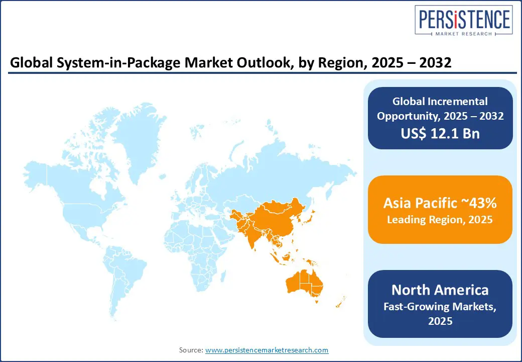
- Asia Pacific region leads the market, with 43% share of global system-in-package, driven by a robust semiconductor ecosystem in China, South Korea, Taiwan, and Japan.
| Global Market Attribute | Key Insights |
| System-in-Package Market Size (2025E) | US$ 13.9 Bn |
| Projected Market Value (2032F) | US$ 26.0 Bn |
| Global Market Growth Rate (CAGR 2025 to 2032) | 9.4% |
| Historical Market Growth Rate (CAGR 2019 to 2024) | 8.5% |
Market Dynamics
Driver - Rising Demand for High Performance Semiconductor Solutions Drives the System-in-Package Market
The global system-in-package market is driven by rising demand for high performance, energy efficient, and compact semiconductor solutions. The rapid growth of AI use in several industries, edge computing, and high speed communications is driving the semiconductor industry.
The governments across the world are encouraging manufacturers to expand their reach through several initiatives, the availability of manufacturing sites, and financial incentives. For instance, in July 2024, the Biden-Harris Administration announced that the U.S. Department of Commerce and Amkor Technology, Inc., signed a non-binding preliminary memorandum of terms to provide up to $400 million in proposed direct funding under the CHIPS and Science Act.
This proposed funding would support Amkor’s investment of approximately $2 billion in a greenfield project in Peoria, Arizona, which will provide full advanced packaging for the world’s most advanced semiconductors for applications in high-performance computing, artificial intelligence, communications, and automotive end markets.
Restraint - High Complexity and Geopolitical Tensions Restrain Market Growth
The system-in-package has a high manufacturing complexity. Its rising production cost is a significant restraint for the market. The technology requires advanced packaging with precise integration of heterogeneous components, increases design challenges, extends production cycles, and elevates costs.
The geopolitical tensions are further hindering the market growth. On April 2, 2025, the U.S. announced reciprocal tariffs on multiple nations, including China. In response, both countries imposed tariffs exceeding 100% on various imported goods for some period, significantly impacting semiconductor supply chains.
Furthermore, China, which is responsible for about 95% of global gallium and germanium production, announced export restrictions on both materials in December 2024. These metals are critical for specific semiconductor processes. The strategic move from China further intensified global supply risks, driving up costs and limiting broader SIP adoption.
Opportunity - AI Expansion and Strategic Focus on Supply Chain Localization Creates Numerous Opportunities
The rising focus on AI-supported systems in different industries, EV adoption, and smart industrial automation is creating an opportunity for the system-in package market. As global economies work to localize semiconductor supply chains, governments are prioritizing advanced packaging as a national asset.
With rising geopolitical trade uncertainties, a focus on secure and domestic semiconductor ecosystems through partnerships and acquisitions is rising among the market players. For instance, in March 2025, AMD announced the completion of its acquisition of ZT Systems, a leading provider of AI and general-purpose compute infrastructure for the world’s largest hyperscale providers.
The acquisition will enable a new class of end-to-end AI solutions based on the combination of AMD CPU, GPU, and networking silicon, open-source AMD ROCm™ software, and rack-scale systems capabilities. It will also accelerate the design and deployment of AMD-powered AI infrastructure at scale, optimized for the cloud.
Category-wise Analysis
Technology Insights
The 3D IC packaging leads the market, with the share of 45%, due to its most advanced and strategically important properties. Its ability to vertically attach multiple dies to create a single, compact, and high performance chip enables high interconnect density, reduced signal latency, and improved thermal and power efficiency. These enhanced properties are highly demanded from several sectors such as AI, data centers, telecommunications, and advanced computing applications.
The manufacturers from various industries are adapting the 3D IC packaging technology to enhance their software. For instance, in April 2025, Synopsys, Inc. announced its ongoing close collaboration with TSMC to deliver robust EDA and IP solutions for TSMC's most advanced processes and advanced packaging technologies to accelerate AI chip design and 3D multi-die design innovation. This collaboration is helping the semiconductor industry speed up the pace of innovation for Angstrom-scale designs by providing mission-critical EDA and IP solutions optimized for the most advanced process technologies. As semiconductor designs continue to scale in complexity, 3D IC packaging offers the scalability and performance required for future innovation.
Method Insights
Flip chip method drives the market growth with a share of 40%, owing to its advanced electrical performance, compactness, and scalability for high density integration. Its direct connection of the die to substrate reduces signal path lengths and improves conductivity, which are mostly preferred in ADAS, AI accelerators, and 5G/6G components.
The market players are investing heavily in the system development by partnering with each other. For instance, in June 2025, at the IEEE Electronic Components and Packaging Technology Conference, Intel unveiled the development of new chip-packaging technology that will allow for bigger processors for AI. The technologies enable the integration of more than 10,000 square millimeters of silicon within a package that can be bigger than 21,000 mm2, a massive area about the size of four and a half credit cards.
As the use of complex systems and performance requirements grows across industries such as automotive, telecommunications, and computing, the market’s dependency on flip chip packaging will increase.
Application Insights
Consumer electronics are dominant accounting for a significant share of 39% in 2025, due to sustained demand for compact, lightweight, and high-performance devices. Smartphones, tablets, smart wearables, and other consumer products are increasingly relying on SIP to integrate sensors, processors, memory, and RF components effectively in a small chip.
The SIP provides the properties that help manufacturers to meet consumer expectations, such as compactness of devices, extended battery life, and faster processing speed. In June 2024, Ansys announced the adoption of NVIDIA Omniverse APIs to offer 3D-IC designers valuable insights from Ansys’ physics solver results through real-time visualization. Ansys is ushering in the next generation of semiconductor system design to improve outcomes in applications including 5G/6G, Internet of Things (IoT), artificial intelligence (AI)/machine learning (ML), cloud computing, and autonomous vehicles. As users demand more advanced features, such as AI featured imaging, voice recognition, and seamless connectivity, SIP technology remains critical for consumer electronics.
Regional Insights
North America System-in-Package Market Trends
The North America system-in-package market is poised to account for a share of 22% of the global industry. It is strengthened by the growing investments in semiconductor independence and an increasing adoption of AI technologies. The region’s market is continuously growing due to the rising demand foAI-baseded features from the defense, automotive, and telecommunication sectors.
The regional government, especially the U.S. government, is supporting the market growth with policies such as the U.S. CHIPS and Science Act. These policies are encouraging the market players to invest in the region to expand their market presence. For instance, in March 2025, TSMC announced its intention to expand its investment in advanced semiconductor manufacturing in the U.S. by an additional $100 billion.
Building on the company’s ongoing $65 billion investment in its advanced semiconductor manufacturing operations in Phoenix, Arizona, TSMC’s total investment in the U.S. is expected to reach US$ 165 billion. The expansion includes plans for three new fabrication plants, two advanced packaging facilities, and a major R&D team center, solidifying this project as the largest single foreign direct investment in U.S. history.
Europe System-in Package Market Trends
The European industry is emerging at a significant rate due to its strong foothold in the automotive, industrial automation, and aerospace sectors. The rise in EV adoption, AI based features in consumer products, as well as in industries is driving the market in the region.
The rising geopolitical tensions and global chip shortages drive the region’s government to reduce its dependency on global supply chains. European Union initiatives, such as the EU Chips Act and national-level funding programs, are promoting market players for the localization of the semiconductor supply chain.
The manufacturers are approaching Europe with expansion strategies. For instance,
- In April 2025, Amkor Technology entered into a strategic partnership with Intel focused on Embedded Multi-Die Interconnect Bridge (EMIB) assembly. This collaboration aims to enhance the availability of the EMIB technology ecosystem and significantly expand advanced packaging capacity in Portugal.
Asia Pacific System-in-Package Market Trends
Asia Pacific dominates the global market with a 43% share, owing to its mature semiconductor domain and a strong demand for AI-based features from the consumer electronics industry. Countries such as China, Taiwan, South Korea, and Japan are increasingly investing in advanced technological developments to support next-generation applications in AI, 5G, and electric mobility.
The leading market players are continuously developing their portfolio to expand their market presence by providing enhanced products. For instance, in July 2024, Samsung Electronics, a world leader in advanced semiconductor technology, announced that it will provide turnkey semiconductor solutions using the 2 nm foundry process and the advanced 2.5D packaging technology Interposer-Cube S (I-Cube S) to Preferred Networks, a leading Japanese AI company.
The rise in geopolitical tensions is driving emerging economies to realign their supply chain system and focus on localization. Export restrictions from China, the dominant global supplier of semiconductor materials, are forcing countries such as Japan, South Korea, Malaysia, and India to diversify their supply chain.
Competitive Landscape
The global system-in-package market is fairly fragmented, driven by rapid innovation, strategic alliances, and government support. The market players are focusing on advanced packaging methods such as 2.5D and 3D integration to meet performance and miniaturization requirements across AI, automotive, and telecommunications sectors. The industry is shifting towards the localization of semiconductor ecosystems, supported by national policies and public funding aimed at enhancing technological self-sufficiency. As global trade tensions and raw material restrictions increase, businesses are relying on supply chain flexibility.
Recent Industry Developments
- In April 2025, TSMC is planning on developing a new chip packaging approach that replaces traditional round substrates with a square substrate. The advanced packaging technology is part of TSMC's broader strategy to cater to the increased power requirements driven by generative AI applications.
- In February 2025, ASE Group officially launched its fifth plant in Penang, which will significantly build on the company’s strong packaging and testing capabilities in the Bayan Lepas Free Industrial Zone. The new plant is part of a strategic expansion plan that will expand the floor space of ASE’s Malaysia facility from its current area of 1 million square feet to approximately 3.4 million square feet.
Companies Covered in System-in-Package Market
- Samsung Electronics
- Amkor Technology
- ASE Group
- AMD
- TSMC
- Intel Corporation
- Fujitsu Ltd.
- Toshiba Electronics
- Qualcomm Inc.
- NXP Semiconductors
Frequently Asked Questions
The system-in-package market growth is set to reach US$ 26.0 Bn by 2032.
The growing demand for compact, power-efficient, and high-performance devices across the consumer electronics and telecom sectors is propelling the system-in-package market growth.
India is estimated to witness a CAGR of 9.5% in the forecast period.
The increasing integration of ADAS and EV components presents a significant opportunity for the system-in-package market.
Samsung Electronics Co., Ltd. is considered the leading player of the system-in-package market.


