


- Advanced Materials
- Pyrolytic Boron Nitride Market
Pyrolytic Boron Nitride Market Size, Share, and Growth Forecast 2025 - 2032
Pyrolytic Boron Nitride Market By Grade (Standard Grade, High Pure Grade, Ultra-Pure Grade), Form (Sheets, Powders, Coatings, Machined Components, Others), Application (Water Processing, OLED, Furnace Components, CSCG, Others), and Regional Analysis for 2025 - 2032
Pyrolytic Boron Nitride Market Size and Trends Analysis
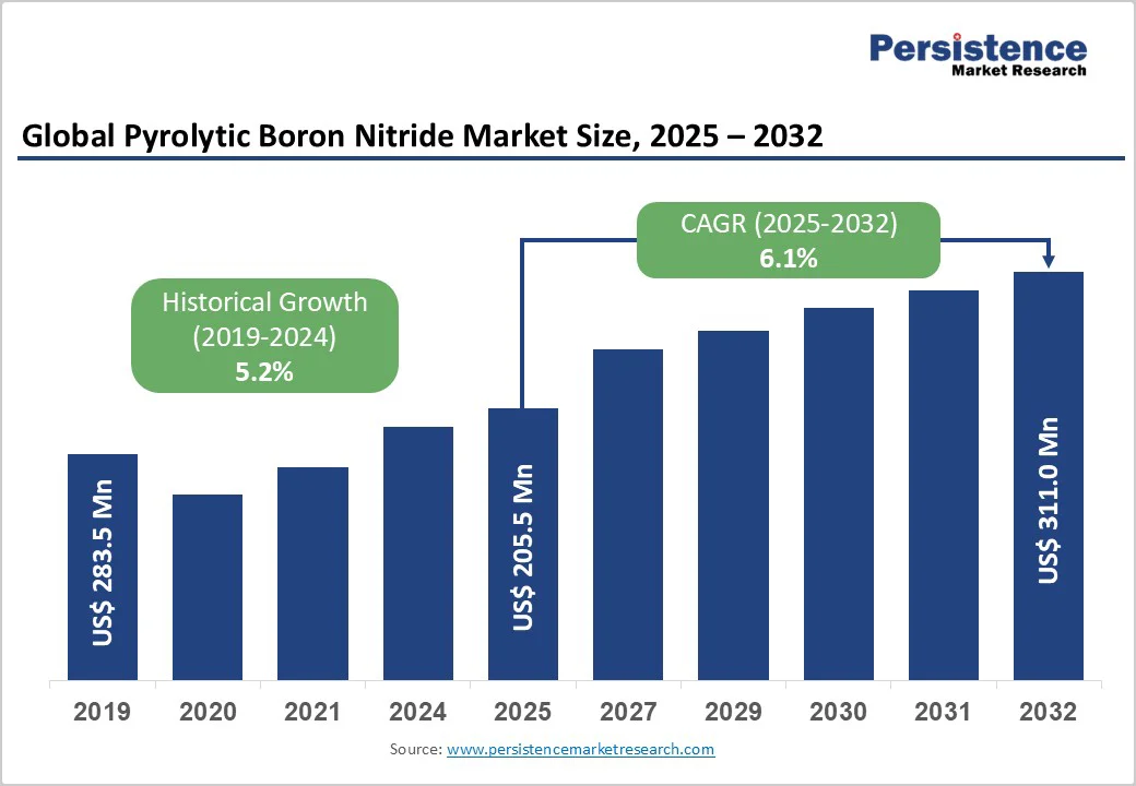
The global pyrolytic boron nitride market is expected to reach US$205.5 million in 2025. It is expected to reach US$311.0 Million by 2032, growing at a CAGR of 6.1% from 2025 to 2032, driven by increasing demand from the semiconductor industry, expanding OLED display manufacturing applications, and the growing need for high-temperature-resistant materials across various industrial applications.
The market benefits from technological advancements in chemical vapor deposition processes and the rising adoption of advanced materials in electronics manufacturing, thermal management systems, and specialized industrial processes.
Key Industry Highlights
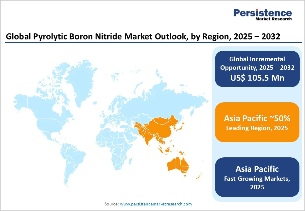
- Leading Region: Asia Pacific emerges as the dominant regional market with 50% global share, driven by semiconductor manufacturing concentration and OLED display production leadership across China, Japan, South Korea, and Taiwan.
- Fastest-Growing Region: China represents the fastest-growing regional market with a 9.7% CAGR through 2030, supported by government semiconductor self-sufficiency initiatives and Made in China 2025 policy investments totaling US$150 Billion.
- Leading Grade Segment: Ultra-pure grade maintains market dominance with 97% segment share, reflecting the critical importance of material purity exceeding 99.99% in semiconductor and OLED manufacturing applications.
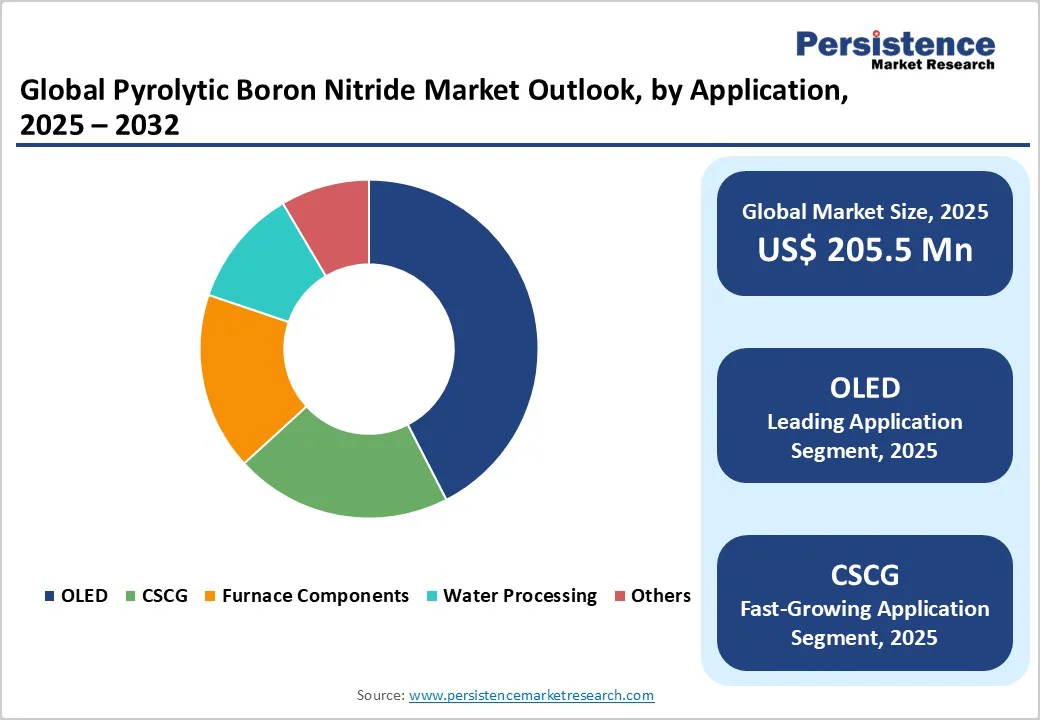
- Fastest-Growing Application Segment: OLED applications constitute the fastest-growing segment, benefiting from global display market expansion projected to reach US$332.9 billion by 2035.
- Key Market Opportunity: Semiconductor crystal growth applications offer the key market opportunity, driven by 5G technology adoption, electric vehicle (EV) expansion, and quantum computing advancements that require ultra-pure materials.
| Key Insights | Details |
|---|---|
| Pyrolytic Boron Nitride Size (2025E) | US$205.5 Mn |
| Market Value Forecast (2032F) | US$311.0 Mn |
| Projected Growth CAGR (2025 - 2032) | 6.1% |
| Historical Market Growth (2019 - 2024) | 5.2% |
Market Factors - Growth, Barriers, and Opportunity Analysis
Growth Analysis - Expanding Semiconductor Manufacturing and Crystal Growth Applications
The global expansion of semiconductor manufacturing, particularly in Asia, is a major driver of demand for pyrolytic boron nitride (PBN). With approximately 70% of global semiconductor production concentrated in Taiwan, South Korea, and China, the region’s reliance on ultra-pure PBN crucibles for compound semiconductor crystal growth, such as GaAs, InP, and GaP, is rapidly increasing.
PBN crucibles, valued at around US$150 million in 2024, are expected to double to nearly US$300 million by 2033. Their exceptional thermal stability and purity (≥99.99%) are indispensable for contamination-free crystal growth in high-frequency semiconductor applications.
The ongoing rollout of 5G technology and demand for next-generation chips amplify this trend. PBN’s compatibility with high-temperature, vacuum, and reactive-gas environments positions it as a preferred material for epitaxy, wafer fabrication, and compound semiconductor growth processes essential to the evolving electronics ecosystem.
Surging OLED Display Market and Thermal Management Applications
The rapid expansion of the OLED display market represents another major growth driver for PBN. Global OLED revenues are projected to surge from US$53.3 billion in 2025 to US$332.9 billion by 2035, marking a CAGR of over 20%. PBN crucibles play a critical role in OLED manufacturing by serving as containers for evaporation sources, where their chemical inertness and high-temperature resistance ensure superior film uniformity and display performance.
Beyond displays, PBN’s applications in thermal management are accelerating as heat dissipation demands rise in 5G devices and EVs. Boron nitride materials can achieve thermal conductivities up to 15 W/m · K when used as polymer fillers, offering excellent dielectric strength (≈80 kV/mm) and a low friction coefficient (<0.3). These properties make PBN a key material for improving reliability and efficiency in advanced electronic and automotive thermal systems.
Barrier Analysis - High Production Costs and Manufacturing Complexity
The pyrolytic boron nitride (PBN) market faces significant restraints due to its highly specialized and costly CVD (Chemical Vapor Deposition) manufacturing process. Production requires extreme conditions, temperatures above 1,800°C and pressures below 1 Torr, demanding advanced equipment and considerable capital investment. Maintaining ultra-pure input gases such as BCl3 and NH3 with impurity levels under 100 ppm adds further expense and technical precision.
PBN’s layered structure introduces handling and fabrication challenges, as internal stresses can lead to delamination, particularly in complex geometries such as VGF crucibles. These factors result in high production costs and limited scalability, restricting widespread adoption compared to lower-cost insulation and refractory materials.
Competition from Alternative Materials and Technical Limitations
PBN encounters growing competition from cost-effective materials such as silicon carbide, graphite, and advanced ceramics, which offer similar thermal conductivity and high-temperature resistance. These substitutes are often preferred in cost-sensitive applications, thereby constraining the penetration of the pyrolytic boron nitride market.
Technical limitations also restrict PBN’s usability. Its anisotropic nature leads to directional variations in mechanical strength and thermal expansion, requiring meticulous design adjustments. The material’s tendency to cleave along layered planes reduces its suitability for applications requiring isotropic mechanical stability, thereby limiting its role in high-stress industrial environments.
Opportunity Analysis - Emerging High-Performance Computing and Quantum Technology Applications
The rapid evolution of high-performance computing (HPC) and quantum computing technologies opens significant opportunities for pyrolytic boron nitride (PBN) manufacturers. HPC environments require materials capable of withstanding extreme heat while maintaining electrical insulation. In this area, PBN excels, with in-plane thermal conductivity reaching 60 W/m·K and electrical resistivity around 10¹? Ω·cm. These attributes make it highly effective for advanced chip packaging, heat spreaders, and substrate insulation applications.
In quantum computing, ultra-pure materials are essential to preserve quantum coherence and minimize interference. PBN’s purity exceeding 99.99% and low outgassing characteristics make it a preferred material for vacuum chambers and cryogenic systems. Increasing public and private investments, such as the U.S. CHIPS and Science Act and Europe’s Quantum Flagship Program, are accelerating material demand, positioning PBN as a critical enabler in next-generation computing ecosystems.
Expansion in Emerging Markets and Advanced Manufacturing Sectors
Expanding semiconductor manufacturing and industrial growth in emerging regions such as Asia-Pacific and Latin America create strong opportunities for PBN adoption. India’s semiconductor sector, for instance, is forecast to grow at 9.7% CAGR through 2030, supported by 75% government funding for new fabs, while China’s “Made in China 2025” initiative, backed by US$150 billion in investments, fuels demand for high-purity materials such as PBN.
Beyond electronics, PBN’s exceptional biocompatibility and stability at temperatures exceeding 1,800°C extend its relevance to aerospace and medical applications. It is increasingly used in pacemaker insulators, artificial heart valve coatings, and jet engine components where thermal endurance and chemical inertness are critical. As the advanced manufacturing and aerospace sectors scale, PBN is poised to gain prominence as a high-performance material for next-generation engineered systems.
Category-wise Analysis
Grade Insights
Ultra-pure grade dominates the pyrolytic boron nitride market with around 97% share, reflecting the critical need for extreme purity in high-performance applications. Purity levels exceed 99.99%, with total metallic impurities below 10 ppm, making it essential for semiconductor manufacturing and OLED processes.
The sophisticated CVD manufacturing process involves precise control of high-purity precursors such as BCl3 and NH3 under extreme conditions. Industry leaders, including Shin-Etsu Chemical and Momentive Technologies, leverage proprietary processes to minimize contamination and ensure consistent quality. The semiconductor sector’s stringent requirements for contamination-free environments further drive preference for ultra-pure PBN, where even trace impurities can impact device yield and performance.
Form Insights
Machined components lead the pyrolytic boron nitride market with roughly 45% share, driven by diverse requirements across semiconductor, OLED, and industrial applications. Crucibles dominate this segment, supporting compound semiconductor crystal growth methods such as CVD and molecular beam epitaxy.
PBN’s machinability allows intricate designs including plates, wafers, tubes, and specialized fixtures, with companies such as Morgan Advanced Materials providing CNC grinding and lapping to tight tolerances. Coatings form another key segment, where PBN films enhance oxidation resistance and extend component life in high-temperature vacuum systems. The ability to maintain structural integrity and precision across complex geometries makes machined PBN components highly valuable for critical applications.
Application Insights
OLED applications hold the largest PBN market share at around 40%, driven by the booming display industry in consumer electronics, automotive, and industrial sectors. PBN crucibles serve as primary evaporation vessels in OLED manufacturing, preventing contamination during the deposition of organic materials.
Semiconductor crystal growth, including compound semiconductor applications, accounts for roughly 35% of the pyrolytic boron nitride market, fueled by demand for III-V semiconductors such as GaAs, InP, and GaN in 5G, automotive, and defense electronics. Furnace components represent 20%, leveraging PBN’s thermal shock resistance and stability above 2000°C for insulators, heating elements, and structural components in high-temperature vacuum furnaces.
Regional Insights
North America Pyrolytic Boron Nitride Trends
North America accounts for approximately 25% of global PBN demand, driven by strong semiconductor manufacturing capabilities and advanced R&D activities. The U.S. hosts leading manufacturers, including Intel, Micron, and Texas Instruments, requiring ultra-pure PBN components for high-performance semiconductor and precision applications. Annual investment in advanced materials exceeds US$600 Billion, fostering the adoption of PBN in laboratories and manufacturing sectors.
The region’s consumer electronics market, valued at US$250.7 Billion in 2024 and growing at a 4.4% CAGR through 2030, further supports demand for PBN in display production and thermal management. Government initiatives such as the CHIPS and Science Act aim to reshore semiconductor manufacturing, enhancing opportunities for domestic PBN suppliers while strengthening supply chain resilience in critical technology sectors.
Europe Pyrolytic Boron Nitride Trends
Europe represents a significant pyrolytic boron nitride market, particularly across Germany, France, the United Kingdom, and Spain, driven by aerospace, automotive, and precision manufacturing applications. Robust regulatory frameworks ensure high-quality standards for advanced materials, while German automotive and precision engineering sectors create strong demand for PBN in high-temperature components and thermal management systems.
The aerospace industry’s focus on high-performance materials boosts PBN adoption for engine components and thermal barriers. Harmonized EU regulations facilitate consistent market access and safety standards for PBN manufacturers. Europe’s emphasis on sustainable production aligns with PBN’s chemically inert and non-toxic properties, supporting growth in environmentally conscious industrial applications.
Asia Pacific Pyrolytic Boron Nitride Trends
Asia Pacific dominates the pyrolytic boron nitride market with roughly 50% share, driven by semiconductor manufacturing, electronics production, and OLED display technologies. China, Japan, South Korea, and Taiwan lead semiconductor capacity, with TSMC and other foundries requiring ultra-pure PBN crucibles for advanced processing. The region accounts for 70% of global LED manufacturing output.
China’s Made in China 2025 policy, with US$150 Billion in investments, supports semiconductor self-sufficiency and drives high-purity PBN demand. Japan’s materials science expertise and South Korea’s memory chip production strengthen market fundamentals. Government subsidies covering up to 75% of fab costs encourage continued expansion, ensuring Asia Pacific remains the largest growth hub for PBN components.
Competitive Landscape
The global pyrolytic boron nitride market demonstrates a moderately consolidated structure, with leading players leveraging technological expertise and advanced manufacturing capabilities to maintain dominance. Key strategies focus on vertical integration, controlling the value chain from raw material sourcing to finished product delivery, ensuring quality, consistency, and supply reliability.
Market differentiation is driven by high purity levels, customization options, and technical support services. Significant R&D investments enhance material properties and manufacturing efficiency, while high entry barriers due to complex production processes and substantial capital requirements maintain market stability and foster continuous innovation among existing participants.
Key Market Developments
- In March 2025, Morgan Advanced Materials (United Kingdom) expanded its CVD production capabilities with new equipment installations targeting increased capacity for PBN crucibles and specialized components, responding to growing demand from the semiconductor industry.
- In September 2024, Shin-Etsu Chemical (Japan) announced the successful development of enhanced PBN coating technologies for CIGS thin-film solar cell applications, demonstrating improved performance characteristics and extended service life.
- In June 2024, Saint-Gobain Ceramic Materials (France) introduced new boron nitride powder formulations optimized for thermal management applications in EV battery systems and 5G telecommunications equipment.
Companies Covered in Pyrolytic Boron Nitride Market
- Shin-Etsu Chemical Co., Ltd.
- Momentive Technologies
- Beijing Boyu Semiconductor (Vessel Craftwork Technology) Co., Ltd.
- Guojing New Material
- Zhejiang Nuohua Ceramic
- CVT GmbH & Co. KG
- Yantai HeFuxiang Ceramics
- Morgan Advanced Materials plc
- Stanford Advanced Materials
- Thermic Edge
- Saint-Gobain Ceramic Materials
- Denka Company Limited
- 3M Company
- ZYP Coatings, Inc.
- Shandong Pengcheng Special Ceramics Co., Ltd.
Frequently Asked Questions
The pyrolytic boron nitride market is projected to reach US$311.0 Million by 2032, growing from US$205.5 Million in 2025 at a CAGR of 6.1% during the forecast period.
Key demand drivers include expanding semiconductor manufacturing requiring ultra-pure materials, surging OLED display market growth projected at 20.1% CAGR, and increasing thermal management needs in 5G telecommunications and EV applications.
Ultra-Pure Grade dominates with approximately 97% market share, driven by stringent purity requirements exceeding 99.99% in semiconductor crystal growth and OLED manufacturing applications.
Asia Pacific holds a 50% share of the global market, driven by its strong semiconductor manufacturing base in Taiwan, South Korea, China, and Japan, along with its leadership in OLED display production.
Major opportunities include emerging high-performance computing and quantum technology applications, expansion in emerging markets such as China and India, and growing aerospace and medical device applications requiring biocompatible, high-temperature materials.
Leading companies include Shin-Etsu Chemical Co., Ltd., Momentive Technologies, Morgan Advanced Materials plc, Saint-Gobain Ceramic Materials, and Denka Company Limited.


