


- Chipsets & Processors
- Atomic Force Microscope Market
Atomic Force Microscope Market Size, Share, and Growth Forecast 2026 - 2033
Atomic Force Microscope Market by Grade (Research Grade AFM, Industrial Grade AFM), by Application (Material Science, Life Sciences, Semiconductors and Electronics, Academics, Others), by Regional Analysis, 2026-2033
Atomic Force Microscope Market Size and Trend Analysis
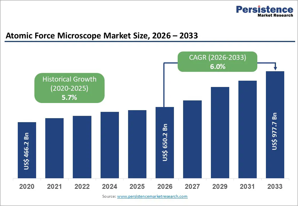
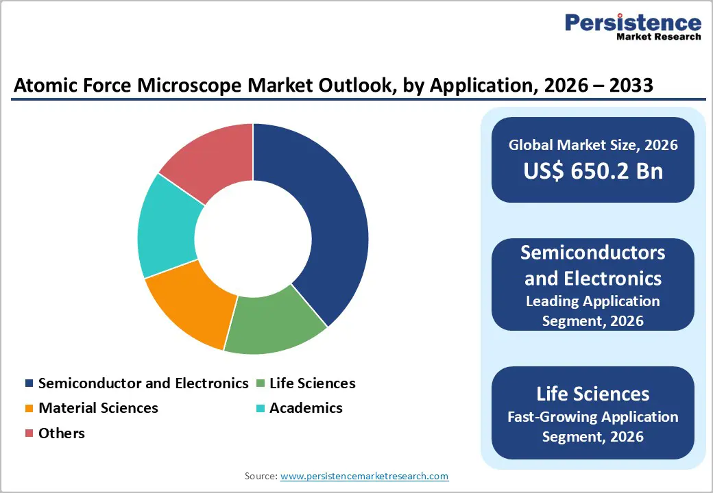
The global atomic force microscope market size is expected to be valued at US$ 650.2 million in 2026 and projected to reach US$ 977.7 million by 2033, growing at a CAGR of 6.0% between 2026 and 2033.
Market growth is primarily driven by accelerating demand for nanoscale surface characterization in semiconductor manufacturing, breakthrough applications in life sciences diagnostics, and substantial global government funding for nanotechnology research.
The semiconductor industry’s relentless pursuit of smaller device geometries and higher integration density requires AFM’s unprecedented nanometer-scale resolution for quality control, defect analysis, and material evaluation. Additionally, increasing investment in biomedical research that uses AFM for cancer cell characterization, protein analysis, and disease diagnostics is expanding the addressable market beyond traditional materials science and industrial metrology into the healthcare and life sciences sectors.
Key Market Highlights
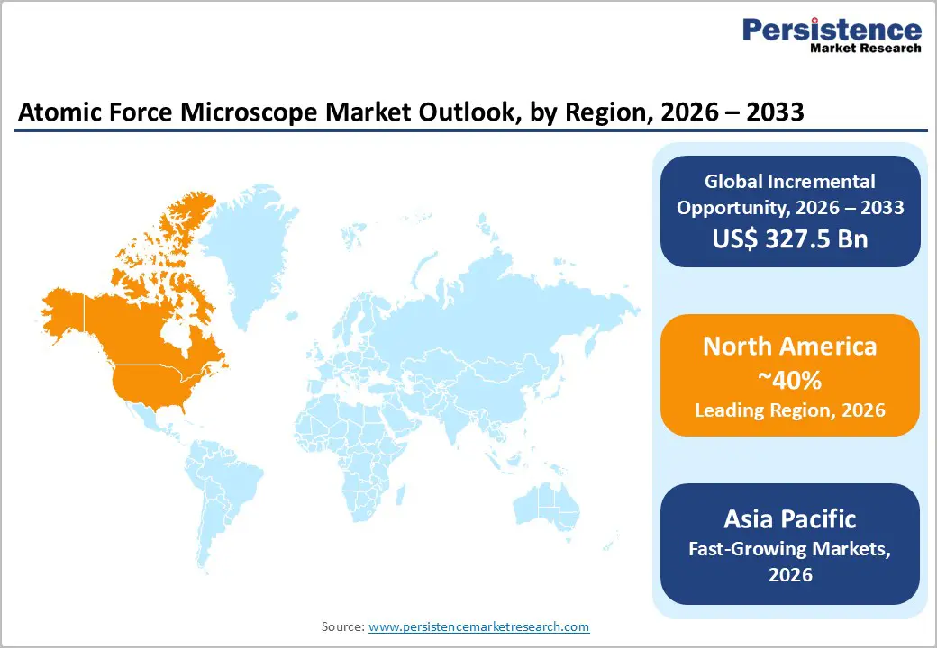
- Leading Region: North America leads the global atomic force microscope market with approximately 40% share in 2025, supported by advanced semiconductor manufacturing, world-class research institutions, substantial government nanotechnology funding, and extensive biomedical research infrastructure.
- Fastest Growing Region: Asia Pacific is the fastest-growing region, expected to post approximately 7.6% CAGR through 2032, driven by China’s semiconductor manufacturing expansion, Japan and Korea’s continued leadership, and growing investment across ASEAN countries in research and advanced manufacturing.
- Dominant Segment: Industrial Grade AFM dominates with roughly 62% share in 2025, driven by essential requirements for quality assurance, process control, and high-precision measurements in semiconductor manufacturing and advanced materials production.
- Fastest Growing Segment: Life Sciences is the fastest-growing application segment, with estimated 8.4% CAGR through 2033, fueled by expanding biomedical research, cancer diagnostics applications, and emerging precision medicine initiatives requiring advanced nanoscale characterization.
- Key Market Opportunity: AI and machine learning integration in AFM data analysis presents significant opportunity for improved productivity, reduced technical expertise requirements, and expanded adoption across research and industrial segments, particularly for semiconductor quality assurance and disease diagnostics applications.
| Key Insights | Details |
|---|---|
| Atomic Force Microscope Market Size (2026E) | US$ 650.2 Mn |
| Market Value Forecast (2033F) | US$ 977.7 Mn |
| Projected Growth (CAGR 2026 to 2033) | 6.0% |
| Historical Market Growth (CAGR 2020 to 2025) | 5.7% |
Market Dynamics
Market Growth Drivers
Semiconductor Industry Expansion and Advanced Device Manufacturing Requirements
The semiconductor manufacturing sector represents the most dynamic growth driver for atomic force microscopy adoption, as chipmakers confront unprecedented technical challenges in device scaling and quality assurance. Modern semiconductor fabrication at sub-5 nanometer technology nodes requires comprehensive nanoscale surface characterization to understand material properties, detect manufacturing defects, and validate thin film characteristics with unprecedented precision. According to the U.S. Department of Commerce, the global semiconductor industry is projected to expand at 8.4% CAGR through 2030, reaching an estimated US$ 1 trillion by 2030, directly amplifying demand for AFM inspection and analysis capabilities.
The Semiconductor Research Consortium reports that AFM techniques, including Conductive AFM (C-AFM), Kelvin Probe Force Microscopy (KPFM), and Scanning Capacitance Microscopy (SCM), are indispensable for semiconductor failure analysis, device performance validation, and process optimization across integrated device manufacturers and foundry operations. Major original equipment manufacturers, including Samsung, TSMC, and Intel, have substantially increased their investments in AFM equipment, recognizing these systems as critical enablers for maintaining manufacturing competitiveness and meeting increasingly stringent quality and performance specifications.
Growth in Life Sciences Research and Biomedical Applications
Life sciences applications are the fastest-growing segment for atomic force microscopy, driven by the technology’s unique capability to characterize biomolecular and cellular properties at nanometer resolution under physiological conditions. Recent breakthrough research published in prestigious journals, including Nature and Science, has demonstrated AFM’s powerful utility for nanoscale characterization of cancer cells, disease diagnostics, and therapeutic monitoring. According to National Institutes of Health funding data, biomedical research expenditures exceeded US$ 41 billion in 2024, with increasing allocations directed toward advanced instrumentation, including AFM systems for cellular mechanics assessment, protein aggregation monitoring, and disease biomarker discovery.
AFM enables quantitative evaluation of cell morphology, stiffness, adhesion properties, and elasticity—parameters that correlate directly with cellular health status and disease progression. Research institutions worldwide are integrating AFM with complementary techniques, including confocal laser scanning microscopy (CLSM) and total internal reflection fluorescence (TIRF) microscopy, to provide comprehensive morphological and mechanical insights into cancer cell biology, neurodegenerative diseases, and infectious disease mechanisms, creating sustained demand for research-grade instruments optimized for biological sample analysis.
Market Restraints
High Capital Investment and Operational Complexity
Atomic force microscope systems represent significant capital investments, with research-grade instruments commanding prices between US$ 300,000 and US$ 800,000, while specialized industrial-grade systems for high-throughput semiconductor applications exceed US$ 1 million. This substantial capital barrier restricts adoption to well-funded research institutions, established semiconductor manufacturers, and specialized service laboratories, constraining addressable market expansion among smaller organizations, academic departments with limited budgets, and emerging market research institutions.
Beyond initial equipment costs, operating AFM systems requires specialized technical expertise, as sample preparation, probe selection, imaging parameter optimization, and data interpretation demand extensive training and experience. The maintenance and calibration requirements further elevate total cost of ownership, with replacement cantilever probes, service contracts, and software licensing adding 15-20% annually to equipment investments, discouraging adoption among budget-constrained organizations despite substantial scientific benefits.
Sample Damage and Technical Limitations in AFM Imaging
Contact-mode AFM imaging, while enabling high-resolution surface characterization, presents inherent risks of sample damage through mechanical tip-sample interactions, particularly problematic for delicate biological specimens, soft polymer materials, and thin film structures. Lateral forces during conventional scanning can alter sample surface properties, cause permanent deformation in soft materials, and damage sensitive biomolecules through mechanical stress. This constraint has driven the development of gentler non-contact and intermittent-contact modes.
Yet, these advanced techniques require more sophisticated instrumentation, extended scanning times, reduced throughput, and more complex data interpretation, limiting applicability in high-volume industrial quality control environments. Additionally, AFM’s limited field of view—typically 100 µm x 100 µm or smaller—and slow scanning speeds necessitate longer analysis time than faster but lower-resolution optical or electron microscopy alternatives, inhibiting adoption in rapid manufacturing quality assurance processes where throughput and speed take priority over resolution.
Market Opportunities
Emerging AI and Machine Learning Integration in AFM Data Analysis
Significant opportunities exist to expand market by integrating artificial intelligence and machine learning into AFM systems and data analysis workflows, enabling greater productivity and broader adoption across research and industrial segments. Recent research published in Advanced Photonics Research has demonstrated that deep learning approaches using convolutional neural networks can deconvolve AFM images, effectively improving spatial resolution beyond the limitations of traditional cantilever probes and enabling more precise nanoscale characterization.
AI-driven automation of image analysis, probe selection optimization, and scanning parameter adjustment could substantially reduce the technical expertise required to operate AFM systems, lowering adoption barriers for smaller institutions and emerging market researchers. Vendors, including Bruker and Park Systems, are investing aggressively in smart AFM controllers with integrated analytics platforms, automated data processing, and intelligent mode selection algorithms, creating value-added capabilities that differentiate premium offerings and support premium pricing in competitive markets. The convergence of AFM with AI-based image reconstruction, automated defect detection, and predictive analytics for semiconductor quality assurance represents a major growth vector, with applications in advanced chip fabrication, nanomaterial characterization, and precision medicine diagnostics significantly expanding the serviceable addressable market.
Healthcare and Clinical Diagnostics Expansion in Disease Characterization
Substantial opportunities are emerging for AFM deployment in clinical and healthcare settings, extending beyond traditional research applications toward actual disease diagnosis, patient risk stratification, and therapeutic response monitoring. Recent publications in leading biomedical journals, including Nature Nanotechnology and ACS Nano, have demonstrated that AFM-derived nanomechanical parameters—including cell stiffness, adhesion forces, and morphological characteristics—strongly correlate with cancer cell aggressiveness, treatment response, and patient survival.
The American Cancer Society’s estimated 1.9 million new cancer diagnoses in 2024 and the growing demand for personalized precision medicine create substantial commercial opportunities for AFM-based diagnostic tools that provide objective, quantitative biomarkers for treatment planning and monitoring. Development of simplified, high-throughput AFM platforms optimized for clinical sample processing, combined with regulatory approvals under FDA guidance documents for companion diagnostic devices, could unlock a major new revenue stream as healthcare systems invest in advanced diagnostic capabilities supporting precision oncology and personalized medicine initiatives. Companies developing integrated AFM-based diagnostic platforms for cancer assessment, infectious disease detection, and cardiovascular risk characterization could capture significant market share in the high-growth clinical diagnostics sector.
Category-wise Insights
Grade Analysis
Within the grade category, industrial-grade atomic force microscope systems hold a dominant position, accounting for nearly 62% of the market share in 2025, driven by their critical role in high-precision, high-throughput industrial environments. These systems are purpose-built for manufacturing applications, featuring superior mechanical stability, thermal control, automation, and integrated data analytics to ensure consistent and repeatable nanoscale measurements. Their indispensable use in semiconductor fabrication for critical dimension measurement, surface roughness analysis, thin-film evaluation, and defect detection firmly anchors demand. Beyond semiconductors, adoption across photovoltaic manufacturing, data storage media, and advanced materials production further supports sustained demand for robust, production-grade AFM systems optimized for continuous industrial operation.
Application Analysis
By application, semiconductors and electronics represent the largest market segment, accounting for approximately 35% share in 2025, reflecting the industry’s heavy reliance on AFM for device development and process control. AFM enables precise evaluation of thin films, interfaces, and nanoscale defects essential for meeting stringent performance and reliability standards. As chipmakers advance toward smaller technology nodes and more complex architectures, the need for ultra-high-resolution surface and dimensional analysis continues to intensify. This structural dependence on nanoscale metrology ensures consistent AFM deployment across fabrication, assembly, and packaging stages, reinforcing the segment’s long-term dominance.
Regional Insights
North America Atomic Force Microscope Market Trends and Insights
North America remains the largest regional market for atomic force microscopes, accounting for around 40% of global demand in 2025, supported by its dominance in semiconductor manufacturing, advanced research infrastructure, and sustained public funding for science and technology. Strong investments in nanotechnology and biomedical research continue to drive consistent demand from universities, national laboratories, and private R&D centers. AFM systems are widely deployed in semiconductor fabrication for critical dimension measurement, surface roughness analysis, and defect inspection, making them integral to advanced process development.
The region also benefits from its leadership in life sciences research, where AFM is increasingly used in cancer research, neuroscience, and molecular-level diagnostics. A well-established ecosystem of equipment suppliers, service providers, and application specialists ensures high system uptime and rapid technology adoption. Regulatory and funding frameworks further encourage procurement of high-performance, premium-grade instrumentation, reinforcing North America’s structurally strong and technology-driven market position.
Europe Atomic Force Microscope Market Trends and Insights
Europe represents a mature and research-intensive market, holding close to 28% share in 2025, underpinned by strong capabilities in materials science, applied physics, and industrial research. Significant funding from pan-European research programs supports advanced manufacturing, nanotechnology, and sustainability-focused innovation, all of which rely heavily on nanoscale characterization tools. The region’s strength in precision engineering and materials research drives extensive adoption of AFM for surface analysis, thin-film characterization, and process optimization.
Academic and applied research institutions across Western Europe form a stable demand base, complemented by industrial users in semiconductors, chemicals, and advanced materials. Harmonized regulatory standards across the European Union promote consistent equipment specifications and quality benchmarks, favoring high-precision, reliable systems. Overall, the European AFM market is characterized by steady demand, long replacement cycles, and a strong preference for technologically advanced instruments aligned with rigorous research and industrial requirements.
Asia Pacific Atomic Force Microscope Market Trends and Insights
Asia Pacific is the fastest-growing regional market for atomic force microscopes, driven by rapid expansion of semiconductor manufacturing, rising R&D expenditure, and increasing focus on technological self-reliance. Large-scale investments in chip fabrication and materials science are significantly boosting AFM adoption for process control, failure analysis, and advanced materials development. Established semiconductor hubs continue to rely on AFM systems as essential tools for nanoscale inspection, while emerging economies are strengthening their research infrastructure across electronics, nanotechnology, and life sciences.
Government-backed programs supporting advanced manufacturing and scientific research are accelerating equipment procurement across academic and industrial laboratories. Additionally, the presence of regional manufacturers offering cost-competitive systems is improving accessibility for smaller research institutes and universities. Combined with growing life sciences research and expanding electronics production, these factors position the Asia Pacific as the primary growth engine for the global AFM market over the coming decade.
Competitive Landscape
The global atomic force microscope market is characterized by a moderately consolidated structure, with a small group of dominant global suppliers and several specialized, niche-focused participants. Leading companies benefit from scale-driven advantages, including extensive global distribution networks, broad product portfolios spanning research and industrial applications, and sustained investments in research and development that support continuous technological upgrades. Competitive positioning increasingly depends on the ability to deliver high-resolution performance, system reliability, and workflow efficiency across diverse end-use environments.
Smaller and mid-sized participants compete through focused differentiation strategies that emphasize application-specific solutions, modular system designs, and close collaboration with academic and industrial customers. Across the market, business strategies are shifting toward automation, AI–enabled data analysis, and advanced imaging modes to reduce operator dependence and improve throughput. Geographic expansion into high-growth regions, particularly in Asia-Pacific, alongside targeted product launches and partnerships, remains a core strategy to strengthen market presence and capture emerging demand.
Key Market Developments
- December 2024: Bruker introduces Dimension Nexus atomic force microscope, an upgradable large-sample AFM with NanoScope 6 controller, PeakForce Tapping, and over 50 modes for high-resolution mechanical property mapping, viscoelastic measurements, and hyperspectral imaging in multi-user labs.
- June 2025: Park Systems hosted global online showcase of Park FX Large Sample AFM Series (FX200, FX300, IR models), demonstrating automated tip exchange, PiFM spectroscopy, and SmartAnalysis for chemical imaging in semiconductor and materials research.
- December 2025: Surfmera unveiled advanced atomic force microscope lineup including AXIS Foundation, Lumina, Proxima, Infra, and Spark. Targeted at materials science, semiconductors, life sciences; features multi-environment control, 50+ modes, AI workflows for precise nanoscale imaging.
Companies Covered in Atomic Force Microscope Market
- Park Systems
- Nanosurf
- Hitachi High-Tech
- NT-MDT Spectrum Instruments
- WITec
- Nanonics Imaging
- NanoMagnetics Instruments
- AFM Workshop
- Bruker
- Attocube Systems
- Semilab
- Nano Scan Technologies
- Horiba
- GETec Microscopy
- Nanoscience Instruments
- Anasys Instruments
- Keysight Technologies
- Leica Microsystems
Frequently Asked Questions
The market is projected to reach approximately US$ 650.2 million in 2026.
Demand is driven by semiconductor industry expansion, growth in life sciences research, large-scale government nanotechnology funding, and emerging biomedical applications.
North America leads the market with around 40% share, supported by strong semiconductor manufacturing and advanced research infrastructure.
Integration of AI and machine learning in AFM systems is the most attractive opportunity for improving productivity and broadening adoption.
Major players include Park Systems, Bruker Corporation, Nanosurf, Hitachi High-Tech, WITec, and NT-MDT Spectrum Instruments.


