


- Plastics, Polymers & Resins
- Thermosetting Moulding Materials for Electronics Market
Thermosetting Moulding Materials for Electronics Market Size, Share, and Growth Forecast 2026 - 2033
Thermosetting Moulding Materials for Electronics Material (Base Material and Competitive Products), Application (Epoxy, Polyester, Polyurethane, Polyimide, Formaldehyde, Bakelite, Others), and Regional Analysis, 2026 - 2033
Thermosetting Moulding Materials for Electronics Market Size and Trend Analysis
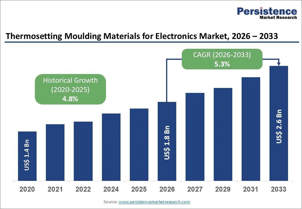
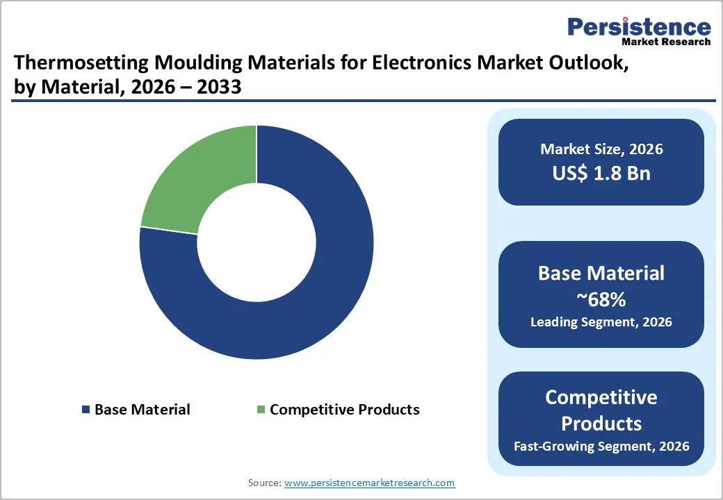
The global thermosetting moulding materials for electronics market size is likely to be valued at US$ 1.8 billion in 2026 and is expected to reach US$ 2.6 billion by 2033, growing at a CAGR of 5.3% during the forecast period from 2026 to 2033.
Market growth is driven by expanding semiconductor manufacturing, the rising adoption of advanced packaging technologies, and increasing demand for high-performance thermosetting materials that support thermal management, insulation, and miniaturized electronics across automotive, consumer, and aerospace applications.
Key Industry Highlights:
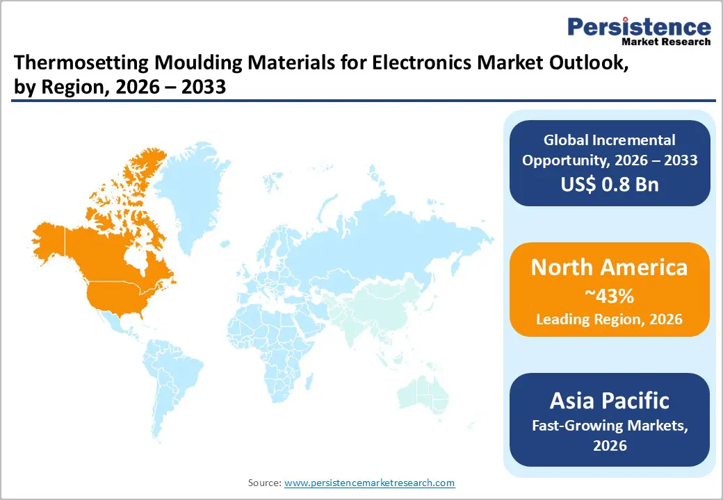
- Leading Region: North America maintains established market dominance, accounting for a 43% share, supported by mature electronics manufacturing, stringent regulatory compliance frameworks, and substantial investment in advanced materials innovation that supports premium product positioning and technology differentiation.
- Fastest-Growing Region: Asia Pacific experiences the fastest regional growth, commanding over 65% of global semiconductor manufacturing capacity, with China expanding at 13.5% CAGR and Taiwan commanding 35.1% of the regional market share, driven by exceptional fabrication capacity expansion and advanced packaging ecosystem development.
- Leading Segment: Epoxy-based thermosetting compounds account for ~40% of the market, driven by exceptional versatility, superior thermal conductivity, electrical insulation, and adhesion properties that support widespread adoption in semiconductor encapsulation and thermal interface applications.
- Fastest-Growing Segment: Advanced semiconductor packaging including flip-chip, fan-out wafer-level packaging, and 3D integration represents fastest-growing segment at 11.3% CAGR, driven by chiplet architectures and AI computing expansion requiring specialized encapsulants and thermal management materials.
- Key Opportunities: Graphene and carbon nanotube-reinforced thermosetting composites enable thermal conductivity improvements up to threefold, while ASEAN manufacturing hub expansion with Penang factory space reaching 3.4 million sq. ft. in 2025 creates substantial opportunity for regional material suppliers and technology integration.
| Key Insights | Details |
|---|---|
| Thermosetting Moulding Materials for Electronics Market Size (2026E) | US$ 1.8 Billion |
| Market Value Forecast (2033F) | US$ 2.6 Billion |
| Projected Growth CAGR (2026 - 2033) | 5.3% |
| Historical Market Growth (2020 - 2025) | 4.8% |
Market Dynamics
Drivers - Semiconductor Industry Expansion and Advanced Technology Node Development Driving Material Demand
The rapid expansion of global semiconductor manufacturing capacity is strongly driving demand for specialized thermosetting moulding materials. The Asia-Pacific region accounts for more than 65% of global semiconductor production, supported by ongoing investments in new fabrication facilities and capacity-expansion projects.
As advanced semiconductor nodes such as 5nm and below become mainstream, material performance requirements have become significantly more stringent. High-purity quartz (HPQ) and advanced thermosetting compounds are increasingly essential for manufacturing equipment, cleanroom systems, and process chambers that must withstand extreme temperatures and aggressive chemical environments.
Semiconductor equipment manufacturers require encapsulants and potting compounds offering high thermal conductivity, low dielectric constants, and minimal shrinkage to ensure stable device performance. These technical requirements support premium pricing and accelerate the adoption of advanced formulations.
Advanced Packaging Technologies and Thermal Management Requirements: Accelerating Material Innovation
The growing adoption of advanced semiconductor packaging technologies is significantly accelerating innovation in thermosetting moulding materials. Packaging formats such as flip-chip, fan-out wafer-level packaging, system-in-package, and 3D integration are becoming standard across high-performance electronics. These technologies require materials with superior mechanical strength, thermal conductivity, and dimensional stability. The packaging segment is projected to grow at a nearly 11.3% CAGR, well above the overall semiconductor materials market's CAGR.
Miniaturization trends and chiplet-based architectures generate high heat density, necessitating advanced thermal management solutions. Epoxy and polyimide composites enhanced with metal oxides, graphene, and carbon nanotubes are increasingly used to achieve thermal conductivity levels up to 10 W/(m·K). Rising demand from consumer electronics, electric vehicles, 5G infrastructure, and high-performance computing is further boosting the adoption of thermally conductive adhesives and encapsulants, ensuring long-term reliability and improved device lifespan.
Restraints - Complex Manufacturing Processes and High Production Costs Limiting Market Penetration
The production of advanced thermosetting moulding materials involves complex manufacturing processes that significantly increase overall costs and limit broader market penetration. High-purity quartz manufacturing requires specialized mining, purification, chemical leaching, and high-temperature treatment processes to eliminate trace metallic impurities such as aluminum, iron, titanium, and lithium. These multi-stage purification steps result in material costs that are substantially higher than conventional alternatives.
Thermosetting resin formulations require advanced synthetic technologies, precise filler dispersion, and rigorous quality control systems. Manufacturers must invest heavily in capital-intensive production facilities, specialized technical expertise, and continuous testing infrastructure. These high operational and development costs create entry barriers, particularly for small manufacturers and cost-sensitive markets.
As a result, adoption remains limited in lower-end electronics applications, while premium formulations are largely concentrated among advanced semiconductor and high-performance electronics producers.
Regulatory Compliance Requirements and Material Compatibility Challenges
Stringent regulatory and compliance requirements present another major challenge for the thermosetting moulding materials market. Manufacturers must comply with multiple global regulations related to VOC emissions, RoHS directives, and environmental safety standards. Meeting these requirements increases formulation complexity and adds additional testing, documentation, and certification costs.
In parallel, material compatibility has become increasingly critical as electronics manufacturing processes grow more complex. Thermosetting materials must perform reliably across diverse substrates, semiconductor architectures, and assembly conditions. Extensive qualification testing is required to ensure compatibility with wafers, packages, and manufacturing equipment.
These qualification cycles are time-consuming and often delay commercial adoption of new materials. For price-sensitive manufacturers, long approval timelines and compliance-related costs act as strong deterrents, slowing market penetration despite growing demand for advanced performance materials.
Opportunity - Next-Generation Advanced Packaging and Artificial Intelligence Electronics Ecosystem Growth
The rapid expansion of artificial intelligence, high-performance computing, and advanced packaging technologies presents a significant growth opportunity for thermosetting material manufacturers. AI accelerators and data center processors require advanced packaging architectures that support high power density, improved thermal dissipation, and enhanced reliability. Demand for organic and ceramic substrates in the Asia-Pacific region alone is projected to reach approximately USD 9.4 billion by 2030, thereby increasing the use of underfill resins, die-attach materials, and thermal interface products.
Chiplet integration and 3D stacking technologies further increase material complexity and value addition. Additionally, the expansion of 5G infrastructure and the rising adoption of electric vehicles and autonomous driving systems are generating strong demand for thermally conductive encapsulants. These mission-critical applications require stable, long-lasting materials capable of maintaining performance under continuous thermal stress, positioning advanced thermosetting solutions as essential components of next-generation electronics ecosystems.
Nanotechnology-Enabled Composite Development and ASEAN Manufacturing Hub Expansion
Nanotechnology-enabled thermosetting composites represent a promising opportunity for material innovation and product differentiation. Graphene- and carbon nanotube-reinforced systems have demonstrated significant improvements in both thermal and electrical conductivity compared to conventional materials. Research indicates that even low filler concentrations can substantially enhance conductivity, supporting premium positioning in high-performance electronics applications. In parallel, the rapid expansion of semiconductor assembly and packaging infrastructure across ASEAN countries is creating strong regional demand.
Manufacturing hubs in Malaysia, Vietnam, and Thailand are attracting global investments due to cost efficiency and supply chain diversification strategies. Malaysia’s Penang backend cluster alone is expected to expand factory space to nearly 3.4 million square feet by 2025. Government incentives, technology parks, and localized material production facilities are enabling faster adoption of advanced thermosetting technologies, thereby supporting long-term growth across Asia-Pacific manufacturing ecosystems.
Category-wise Analysis
Material Insights
Base material dominates the thermosetting moulding material, material segment, accounting for approximately 68% of total market share. This leadership is driven by strong demand from semiconductor manufacturing, where ultra-high purity materials exceeding 99.99% SiO2 are essential for device performance and yield stability. HPQ plays a critical role in silicon wafer production through the Czochralski process, quartz crucible manufacturing, and cleanroom equipment applications.
Grade I HPQ commands premium pricing due to its extremely low metallic contamination levels, while Grade II and Grade III variants offer more cost-effective options for less demanding applications. These graded offerings enable suppliers to address a wide range of customer requirements. Alternative materials such as fumed silica, synthetic silica, fused silica, and crystal silica collectively account for nearly 35% market share, providing performance flexibility and cost advantages in applications outside ultra-pure semiconductor environments.
Application Insights
Epoxy resin systems represent the largest application segment, accounting for approximately 40% of the global thermosetting moulding materials market. Their dominance is supported by excellent adhesion strength, electrical insulation properties, dimensional stability, and thermal performance across semiconductor and electronics applications.
Epoxy formulations enhanced with metal oxides, boron nitride, and carbon-based fillers are increasingly used to improve heat dissipation in advanced packaging structures. Polyester resins account for approximately 20% of the market and are widely used in consumer electronics due to their flexibility, toughness, and cost efficiency.
Polyimide-based systems account for approximately 12% of the market and are primarily used in high-temperature environments exceeding 300°C, including aerospace, defense, and advanced electronics. These systems command premium pricing due to their exceptional thermal stability. Phenolic, formaldehyde, and melamine-based resins collectively serve niche applications requiring rigidity, electrical insulation, and rapid curing for high-volume production.
Regional Insights
North America Thermosetting Moulding Materials for Electronics Trends
North America remains a key market for thermosetting moulding materials, supported by a strong semiconductor design ecosystem and advanced electronics manufacturing base. The United States continues to drive demand through investments in artificial intelligence, cloud computing, and 5G infrastructure. These applications require high-performance encapsulants and thermal interface materials capable of managing elevated power densities.
Regulatory frameworks emphasizing environmental protection, product safety, and low-VOC formulations have encouraged innovation in eco-friendly material solutions. This regulatory environment benefits suppliers offering sustainable and high-performance formulations. Major regional players, including BASF and Eastman Chemical, continue to invest heavily in research and development focused on thermal conductivity enhancement and advanced composite technologies. As a result, North America remains a global innovation hub, supporting premium product development and long-term market stability.
Europe Thermosetting Moulding Materials for Electronics Trends
Europe maintains a strong position in the thermosetting moulding materials market due to its advanced automotive electronics and industrial manufacturing sectors. Countries such as Germany, the United Kingdom, France, and Spain generate consistent demand for materials with high thermal stability and regulatory compliance. Germany’s leadership in electric vehicle development and autonomous driving technology is a major growth driver.
Power electronics modules, battery management systems, and control units require thermally conductive encapsulants capable of operating reliably under harsh conditions. European regulatory harmonization has introduced strict standards related to recyclability, biodegradability, and VOC emissions. These policies are encouraging manufacturers to develop bio-based resins and environmentally responsible formulations. Suppliers able to combine sustainability with performance gain a competitive advantage, strengthening Europe’s position as a premium and regulation-driven materials market.
Asia Pacific Thermosetting Moulding Materials for Electronics Trends
Asia-Pacific is the largest and fastest-growing regional market for thermosetting moulding materials, driven by its dominant role in global semiconductor manufacturing. Over 65% of global fabrication capacity is concentrated across China, Taiwan, Japan, and South Korea. China continues to expand at a CAGR of 4.1%-13.5%, driven by government incentives, domestic sourcing initiatives, and large-scale fab construction projects.
Taiwan remains a regional leader, accounting for over 35% of Asia-Pacific semiconductor materials demand due to its dense ecosystem of foundries and advanced packaging providers. Meanwhile, ASEAN countries are rapidly strengthening backend assembly and testing capabilities. Localized material production reduces logistics costs and enhances supply chain resilience, supporting sustained adoption of thermosetting encapsulants and thermal management materials across the region.
Competitive Landscape
The global thermosetting moulding materials for electronics market exhibits moderate consolidation, with a mix of multinational chemical companies and specialized regional suppliers. Tier 1 manufacturers such as BASF SE, Evonik Industries, Eastman Chemical Company, and Ashland Global Holdings collectively account for the larger global market share. Their dominance is supported by extensive product portfolios, global manufacturing footprints, and strong customer relationships.
Regional specialists and emerging technology providers hold around 20-25% market share by focusing on niche applications such as high thermal conductivity materials, nanocomposites, and sustainable formulations. Competitive strategies increasingly emphasize research and development investment, process automation, and advanced molding technologies. Sustainability-focused innovation, including self-healing materials and eco-friendly composites, is becoming a key differentiation factor, enabling premium pricing and long-term competitive positioning.
Key Developments:
- In December 2024, BASF SE announced the development of a next-generation epoxy thermosetting composite integrated with graphene nanoparticles, achieving thermal conductivity above 8 W/(m·K). The innovation supports efficient heat dissipation in advanced semiconductor packaging and high-performance computing applications.
- In September 2024, Evonik Industries AG expanded its high-temperature polyimide resin manufacturing facilities in Singapore and China to address rising demand from aerospace electronics and advanced semiconductor applications requiring continuous thermal stability above 300°C.
- In June 2024, Eastman Chemical Company launched a bio-based thermosetting encapsulation material designed to support sustainability goals while delivering thermal and electrical performance comparable to traditional petrochemical-based resins used in electronics manufacturing.
Companies Covered in Thermosetting Moulding Materials for Electronics Market
- BASF SE
- Evonik Industries AG
- Eastman Chemical Company
- Cosmic Plastics Inc.
- Chang Chun Plastics Co. Ltd.
- Ashland Global Holding Inc.
- Unimin-Sibelco
- Golovach Quartz
- The Quartz Corporation
- Tosoh Corporation
- ANZAPLAN GmbH
- HPQ Silicon Resources Inc.
- Nordic Mining ASA
- CB Minerals
- Huntsman Corporation
- Momentive Performance Materials
- Kolon Industries
- KYOCERA Corporation
Frequently Asked Questions
The global market is expected to reach US$ 2.6 billion by 2033, growing at a 5.3% CAGR driven by semiconductor, AI, IoT, and 5G expansion.
Market growth is driven by semiconductor capacity expansion, advanced packaging technologies, and rising thermal management needs in miniaturized electronics.
Epoxy resins lead the market with around 40% share due to strong thermal performance, electrical insulation, and wide use in electronics encapsulation.
Asia Pacific dominates the market, supported by over 65% of global semiconductor manufacturing capacity and strong advanced packaging ecosystems.
Major opportunities include AI-driven advanced packaging growth and nanotechnology-based composites offering enhanced thermal conductivity.
Key players include BASF SE, Evonik Industries AG, Eastman Chemical Company, Ashland Global Holdings, and Cosmic Plastics Inc.


