


- Semiconductor Materials & Components
- Manual Wafer Aligner Market
Manual Wafer Aligner Market Size, Share, and Growth Forecast 2026 - 2033
Manual Wafer Aligner Market by Product Type (Standard Manual Wafer Aligners, High-Precision Manual Wafer Aligners, Customized Manual Wafer Aligners), by Wafer Size (≤100 mm, 101-200 mm, 201-300 mm, 300 mm), Application (Front-End Wafer Fabrication, Back-End Packaging, Assembly & Testing, Research & Development, Educational Applications), End-User, Regional Analysis, 2026 - 2033
Manual Wafer Aligner Market Size and Trend Analysis
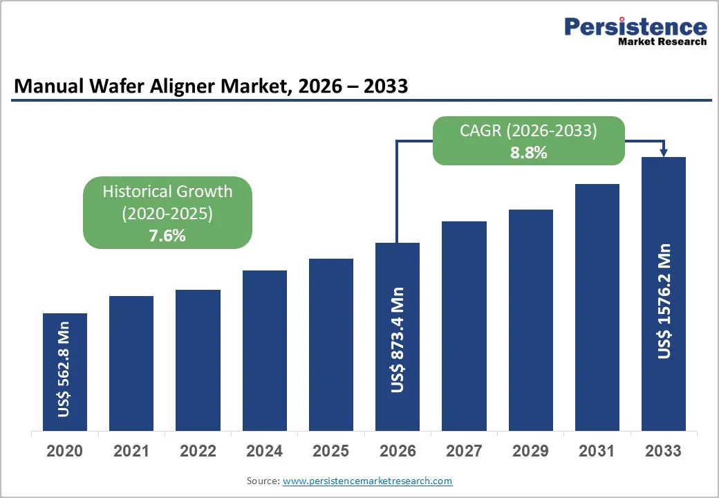
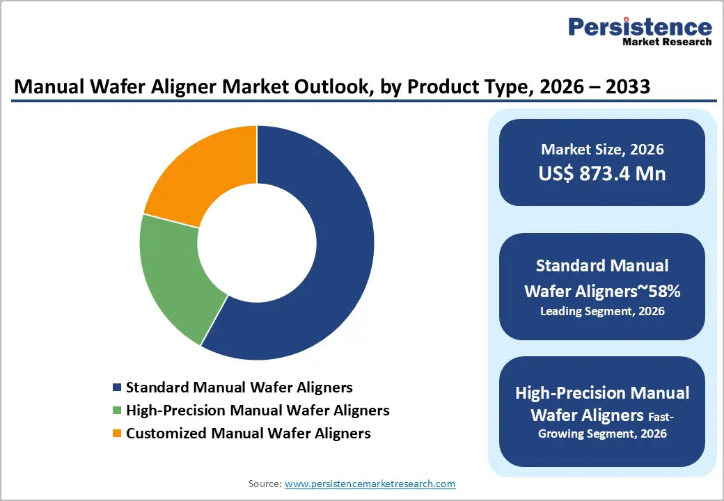
The global manual wafer aligner market size is likely to be valued at US$ 873.4 million in 2026 and is expected to reach US$ 1,576.2 million by 2033, growing at a CAGR of 8.8% during the forecast period from 2026 to 2033.
Market expansion is fundamentally driven by the enduring demand for cost-effective wafer positioning solutions in specialty semiconductor manufacturing, research institutions, and small- to medium-scale production facilities that prioritize operational flexibility over automated throughput.
Key Industry Highlights:
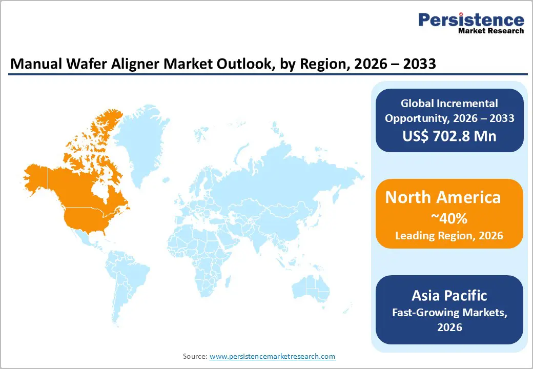
- Leading Region: North America is the leading region, holding 40% share, due to strong semiconductor R&D infrastructure, advanced equipment manufacturing capabilities, high technology adoption, and continuous investment in specialty and research-driven chip production.
- Fastest-Growing Region: Asia-Pacific is the fastest-growing region, with a 10% CAGR, driven by China's 7.6% expansion, India's comparable growth, and ASEAN semiconductor hub development, anchored by foreign direct investment and localization policies.
- Dominant Segment: Standard Manual Wafer Aligners capture 58% market share, reflecting proven reliability, SEMI-compliance, broad 75-200mm wafer size compatibility, and cost-effectiveness supporting diverse semiconductor manufacturing applications.
- Fastest-Growing Segment: 200mm wafer alignment grows at the fastest 10% CAGR, driven by sustained automotive electronics demand, MEMS expansion, growth in power device manufacturing, and unexpected 200mm fab capacity utilization in mature-node production.
- Key Market Opportunity: Asia-Pacific semiconductor localization presents substantial growth potential, with China and India establishing specialized manufacturing, ASEAN hub development, and government-supported fab construction, generating 65% of incremental growth by 2033.
| Key Insights | Details |
|---|---|
| Manual Wafer Aligner Market Size (2026E) | US$ 873.4 Million |
| Market Value Forecast (2033F) | US$ 1,576.2 Million |
| Projected Growth CAGR (2026 - 2033) | 8.8% |
| Historical Market Growth (2020 - 2025) | 7.6% |
Market Dynamics
Drivers - Manual wafer aligners offer cost-efficient, flexible, and reliable solutions for specialty semiconductor production with diverse wafer materials
Manual wafer aligners offer significant cost advantages over fully automated alignment systems, making them highly attractive for specialty semiconductor manufacturing. These systems typically cost 70% less than automated platforms while still delivering reliable positioning accuracy of ±0.5-1.0 micrometers. As a result, manufacturers producing MEMS devices, automotive-grade power semiconductors, and compound semiconductors increasingly prefer manual aligners for low- to mid-volume production.
The absence of complex robotics, advanced programming, and high maintenance requirements significantly reduces operational costs and technical complexity. At the same time, manual systems offer greater flexibility in handling various wafer sizes, materials, and substrates. They can process InP, GaAs, GaN, and SiC wafers without requiring expensive reconfiguration. This adaptability makes manual wafer aligners ideal for specialty fabs with frequently changing product portfolios, helping manufacturers balance precision, flexibility, and cost efficiency.
Sustained reliance on mature-node technologies continues driving strong demand for manual wafer alignment in 200mm semiconductor fabs
The 200mm wafer segment holds 42.1% of total market revenue and remains a key growth driver for manual wafer aligners. Contrary to earlier expectations of decline, 200mm fabs continue to operate at high utilization due to strong demand from automotive, industrial, and telecommunications sectors. These industries rely heavily on mature-node semiconductors known for reliability, long lifecycles, and cost efficiency.
Manual wafer aligners are well-suited to 200mm processing, offering sufficient precision while avoiding the high capital investment associated with 300mm automated infrastructure. Automotive electronics production alone exceeds US$50 billion annually, driving a sustained demand for power devices, analog chips, and MEMS sensors manufactured on 200mm wafers. The continued use of legacy nodes in analog devices and industrial applications sustains stable demand for SEMI-compliant manual alignment equipment designed specifically for 200mm cassette handling and mature fabrication environments.
Restraints - Rising adoption of AI-enabled automated alignment systems limits manual wafer aligner usage in high-volume and advanced-node manufacturing
Automated wafer alignment systems are increasingly competing with manual equipment, particularly in high-volume semiconductor manufacturing. Advanced systems equipped with AI-based vision technology, robotics, and predictive analytics deliver significantly higher throughput. Automated platforms can complete wafer alignment cycles in under 10 seconds, compared with 30 seconds for manual systems, resulting in a 400% increase in productivity. Large semiconductor manufacturers producing advanced-node chips increasingly mandate fully automated wafer handling across their fabs.
Industry 4.0 requirements such as real-time process monitoring, predictive maintenance, and MES integration strongly favor automated solutions. Manual systems often lack native digital connectivity, limiting their suitability for smart factory environments. As semiconductor fabs continue prioritizing efficiency, traceability, and automation, the adoption of fully automated alignment equipment reduces opportunities for manual systems in premium and high-throughput production settings.
Precision constraints and operator dependency restrict manual wafer aligner suitability for advanced lithography and high-throughput semiconductor environments
Manual wafer aligners are constrained by technical limitations that limit their use in advanced semiconductor manufacturing. Operator-dependent alignment introduces variability, typically limiting accuracy to ±0.5-1.0 micrometers. While sufficient for mature-node processes, this level of precision is inadequate for advanced lithography and packaging applications requiring sub-100-nanometer accuracy. In high-volume production environments, manual operation also limits throughput and consistency, making it unsuitable for 300mm fabs processing millions of wafers annually.
These facilities require continuous wafer flow and fully automated handling systems to meet productivity targets. Additionally, semiconductor startups in developing regions often face capital constraints that limit investment in equipment upgrades and advanced tooling. These factors collectively constrain the scalability of manual wafer aligners, slowing adoption in advanced fabrication environments and limiting their use primarily to specialty, research, and mature-node manufacturing applications.
Opportunity - Rapid semiconductor localization and government-backed manufacturing expansion in Asia-Pacific create strong growth opportunities for manual wafer aligners
Asia-Pacific presents significant growth opportunities for the manual wafer aligner market, driven by semiconductor localization initiatives and rapid industrial expansion. China is growing at a 7.6% CAGR, supported by government policies aimed at reducing dependence on imported chips and strengthening domestic manufacturing. The country targets semiconductor revenues exceeding RMB 500 billion by 2030, with a strong focus on analog devices, MEMS, and mature-node logic manufacturing. India is also emerging as a promising market, supported by government incentive programs encouraging fab development and domestic equipment manufacturing.
ASEAN countries such as Vietnam and Thailand are establishing electronics manufacturing hubs through foreign investment. Manual wafer aligners are particularly well suited to these regions due to their lower capital costs, simpler operation, and minimal infrastructure requirements. These advantages make them ideal for startups and regional manufacturers seeking to build initial production capabilities with limited investment budgets.
Expanding MEMS, optoelectronics, solar, and research applications significantly increase demand for flexible and cost-effective manual wafer alignment systems
The expansion of MEMS, optoelectronics, and emerging semiconductor applications is creating strong demand for manual wafer aligners. The global MEMS market is projected to grow at an annual rate of 12% through 2030, driven by increasing adoption in automotive sensors, industrial monitoring, and consumer electronics. These applications often require flexible equipment capable of handling compound semiconductors and non-standard substrates. Similarly, LED and display manufacturing continues to grow at 7% annually, particularly in automotive lighting and advanced display technologies using GaN substrates.
Photovoltaic manufacturing is expanding at an even faster rate, with 15% annual growth driven by perovskite and tandem solar cell technologies that require precise yet adaptable wafer handling. Additionally, universities and research institutions worldwide are establishing semiconductor laboratories focused on photonics, nanotechnology, and quantum research. These facilities favor affordable, flexible manual alignment systems for experimental and educational use.
Category-wise Analysis
Product Type Insights
Standard manual wafer aligners dominate the market with a 58% share, supported by proven reliability, mature supply chains, and broad compatibility with existing fabrication infrastructure. These systems typically provide ±0.5-1.0 micrometer alignment accuracy, sufficient for most specialty and mature-node semiconductor processes. They support multiple wafer sizes, including 75mm, 100mm, 150mm, and 200mm, enabling versatile use across diverse applications. Standard aligners incorporate features such as spring-loaded notch detection, antistatic roller systems, and ESD protection to ensure safe wafer handling in ISO 4 cleanroom environments.
Their SEMI-compliant design allows seamless integration with industry-standard cassettes, reducing qualification time and installation complexity. Manufacturers benefit from standardized production designs, enabling cost-efficient manufacturing and competitive pricing. This affordability makes standard manual wafer aligners highly attractive to research institutions and cost-sensitive specialty semiconductor manufacturers.
Wafer Size Insights
Wafers ranging from 101-200 mm account for 42.1% of the total market share, representing the most suitable size range for manual wafer alignment. The 200mm segment offers an optimal balance between manageable precision requirements and cost efficiency. These wafers support a wide range of applications, including automotive electronics, power devices, analog ICs, and MEMS sensors. Across the Asia-Pacific, Europe, and North America, many 200mm fabs continue to operate at high utilization rates due to strong demand for mature-node components.
Unlike 300mm fabs, which require heavy automation investment, 200mm lines allow greater flexibility and lower operating costs. Manual aligners designed to meet SEMI standards and 200mm cassette specifications integrate easily into existing production environments. The long lifecycle of mature-node technologies ensures continued reliance on 200mm wafers, sustaining steady demand for manual alignment systems in specialty semiconductor manufacturing.
Application Insights
Front-end wafer fabrication accounts for 64% of total demand, making it the largest application segment for manual wafer aligners. These systems play a critical role in lithography, deposition, and etching processes by ensuring accurate wafer orientation prior to processing. Manual aligners are especially important for non-EUV lithography widely used in mature-node and specialty semiconductor production. Back-end packaging applications account for 18% of demand, including wafer preparation for dicing, bumping, and assembly, where correct orientation and lot verification are essential.
Research and development applications contribute 12% of market demand, driven by academic institutions and corporate R&D centers. These environments require flexible equipment capable of supporting experimental materials, new device structures, and prototype manufacturing. The adaptability and affordability of manual wafer aligners make them particularly valuable in R&D settings focused on innovation rather than mass production efficiency.
End-user Insights
Semiconductor manufacturing accounts for 76% of end-user demand, primarily driven by specialty semiconductor producers and mature-node fabs. These manufacturers prioritize cost efficiency, operational flexibility, and reliability over full automation. MEMS and sensor manufacturers account for 12% of demand, driven by rising adoption of sensors in automotive safety systems, industrial automation, and consumer electronics. Optoelectronics accounts for 5%, including manufacturers of laser diodes, photodiodes, and optical components requiring accurate wafer alignment for heterogeneous integration.
LED and display manufacturing accounts for 4% of total demand, driven by growth in automotive lighting and advanced display technologies. Research institutes and universities account for the remaining 3%, reflecting continued investment in semiconductor education and advanced research. These institutions rely on manual wafer aligners for their affordability, ease of operation, and support for diverse experimental substrates and processes.
Regional Insights
North America Manual Wafer Aligner Market Trends
North America maintains a strong presence in the manual wafer aligner market, supported by advanced research infrastructure and an established specialty semiconductor manufacturing sector. The U.S. semiconductor industry, valued at over US$ 200 billion annually, includes significant production of analog devices, power semiconductors, and MEMS components that rely on manual alignment systems for research and low-volume manufacturing. However, overall market growth remains moderate due to industry maturity and increasing consolidation toward automated large-scale fabs.
Universities and research laboratories remain major purchasers, using manual wafer aligners for training programs and experimental research. To remain competitive, equipment manufacturers in North America are enhancing manual systems with digital features, including data logging, process monitoring, and software connectivity. These upgrades help align traditional manual equipment with modern fab requirements while preserving cost and operational simplicity.
Europe Manual Wafer Aligner Market Trends
Europe accounts for approximately 28% of global market share, led by Germany, which holds 32.1% of the regional market. The country benefits from strong precision-engineering capabilities and a well-established semiconductor-equipment manufacturing base. Germany remains a global leader in wafer handling and positioning technologies. France, the UK, and Spain contribute to steady demand, particularly in defense, automotive, and pharmaceutical semiconductor applications that require MEMS and specialty devices.
European manufacturers emphasize high quality, regulatory compliance, and customization to meet diverse application requirements. The regional market grows at a 5.1% CAGR, reflecting its maturity. Industry focus is increasingly shifting toward integrated solutions that support Industry 4.0 adoption, process traceability, and regulatory harmonization across EU member states, strengthening long-term demand for advanced yet flexible manual alignment systems.
Asia Pacific Manual Wafer Aligner Market Trends
The Asia-Pacific region is the fastest-growing market, driven by rapid industrialization and strong government support for semiconductor manufacturing. China is expanding at a 7.6% CAGR, investing heavily in domestic production of analog devices, power semiconductors, and MEMS components. India is exhibiting similar growth momentum through government incentive programs that promote fab development and local equipment manufacturing. Japan maintains a stable demand, particularly in research institutions and specialty device manufacturing.
ASEAN countries, such as Vietnam, Thailand, and Indonesia, are emerging as electronics manufacturing hubs, supported by foreign direct investment. The region benefits from cost-competitive manufacturing, expanding technical talent, and supply chain localization strategies. Manual wafer aligners are well-suited to these markets due to their affordability and operational simplicity. The Asia-Pacific region is expected to account for 65% of incremental market growth through 2033, driven by regional manufacturing expansion and localization initiatives.
Competitive Landscape
The manual wafer aligner market is moderately fragmented, with the top 15 manufacturers accounting for the largest share of global revenue. This structure reflects balanced competition between established global players and emerging regional suppliers. Leading companies such as Emu Technologies, SPS-International, and GL Automation benefit from strong installed bases, long-term customer relationships, and proven manufacturing expertise. Meanwhile, emerging manufacturers from China and India, including Chung King Enterprise, Dou Yee Enterprises, and Shen-Yueh Technology, focus on cost-competitive offerings targeting price-sensitive customers.
Competitive strategies emphasize customization, regional expansion, and strong after-sales support. Innovation efforts increasingly focus on digital monitoring, improved alignment precision, and compatibility with compound semiconductor materials. Vertical integration enables suppliers to offer bundled wafer-handling solutions. New business models, including equipment leasing and service-based partnerships, are also gaining traction to address capital constraints faced by semiconductor startups.
Key Developments:
- In November 2024, Emu Technologies introduced an improved 200 mm manual wafer aligner featuring enhanced anti-vibration mechanisms and robust ESD protection designed to meet precision alignment needs for mature-node specialty semiconductor production environments. This upgrade improves alignment accuracy while maintaining cost-effectiveness for specialty fabs.
- In July 2024, SPS-International expanded its product portfolio to include manual wafer alignment systems tailored for MEMS and compound semiconductor applications. These systems support substrates such as GaN, InP, and GaAs, with specialized positioning features that optimize accuracy and process flexibility across a range of materials in cleanroom environments.
- In April 2025, several Chinese manufacturers increased their combined annual manual wafer aligner production capacity to more than 50,000 units, aiming to capitalize on cost-competitive manufacturing and growing regional semiconductor demand, particularly in Asia-Pacific markets, by expanding domestic equipment supply and focusing on mature semiconductor segments.
Companies Covered in Manual Wafer Aligner Market
- Emu Technologies
- SPS-International
- GL Automation
- H-Square
- G2 Automated Technologies
- Chung King Enterprise
- Dou Yee Enterprises
- Honwe Precision
- Shen-Yueh Technology
- Standard Technology
- Chain-Logic International
- Suzhou SOSCH Microelectronics
- JEL Corporation
- Logosol, Inc
- TB-Ploner GmbH
- MGI AUTOMATION
- UST Co., Ltd
- Hon We Precision Co. Ltd
- RECIF Technologies
Frequently Asked Questions
The global Manual Wafer Aligner market is projected to reach US$ 1,576.2 Million by 2033 from US$ 873.4 Million in 2026, growing at a CAGR of 8.8% driven by specialty semiconductor manufacturing expansion, 200mm wafer demand, MEMS growth, and Asia-Pacific industrialization.
Primary drivers include cost-effectiveness versus automated systems, sustained 200mm wafer processing demand representing 42.1% of market share for automotive and mature-node production, MEMS and sensors growth, optoelectronics expansion, Asia-Pacific semiconductor localization at 7.6% CAGR in China, and research institution equipment demand.
Standard Manual Wafer Aligners dominate with 58% market share, reflecting proven reliability, SEMI-compliance, broad 75-200mm wafer size compatibility, established supply chains, and cost-effectiveness supporting diverse semiconductor applications across specialty manufacturers and research facilities.
Asia-Pacific dominates with fastest growth at 7.6% CAGR in China and comparable expansion in India, driven by semiconductor localization, specialty fab establishment, government support programs, ASEAN manufacturing hub development, and cost-competitive production positioning region for 65% of incremental growth through 2033.
200mm wafer segment expansion and Asia-Pacific localization represent primary opportunities, with 200mm fabs growing 10% CAGR supporting automotive electronics, MEMS, and power device manufacturing, combined with semiconductor localization initiatives in China, India, and ASEAN nations requiring cost-effective precision equipment establishing regional production capabilities.
Leading companies include Emu Technologies, SPS-International, GL Automation, H-Square, G2 Automated Technologies, Chung King Enterprise, and Honwe Precision, with top 15 manufacturers controlling largest share of global revenue through established customer bases, manufacturing expertise, and regional market presence.


