




- Semiconductor Materials & Components
- Interposer and Fan-out WLP Market
Interposer and Fan-out WLP Market Size, Share, and Growth Forecast 2026 - 2033
Interposer and Fan-out WLP Market by Packaging Type (Interposer Packaging, Fan-out Wafer-Level Packaging), Interposer Material (Silicon, Organic, Glass, Ceramic), Packaging Architecture (2.5D Packaging, 3D Packaging), End-Use Industry (Consumer Electronics, IT and Telecommunications, Automotive, Industrial Manufacturing, Healthcare and Medical Devices, Aerospace and Defense, Others), and Regional Analysis for 2026 - 2033

Interposer and Fan-out WLP Market Size & Trends Analysis
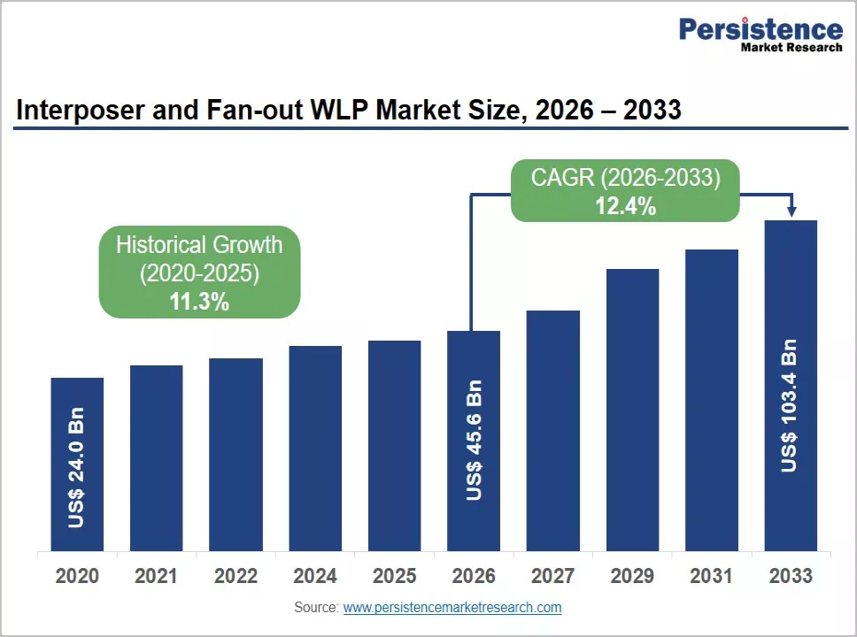
The global interposer and fan-out WLP market is expected to be valued at US$ 45.6 billion in 2026 and is projected to reach US$ 103.4 billion by 2033, expanding at a CAGR of 12.4% during the forecast period. Market growth is driven by increasing demand for artificial intelligence processors, high-bandwidth memory, and compact consumer electronics.
Semiconductor manufacturers are increasingly adopting advanced packaging technologies to improve chip performance, interconnect density, and power efficiency. Advancements in chiplet integration, heterogeneous packaging, and next-generation interposer materials are further supporting semiconductor innovation. Growing investments in data centers, high-performance computing, and advanced semiconductor manufacturing are expected to accelerate global market expansion.
Key Industry Highlights
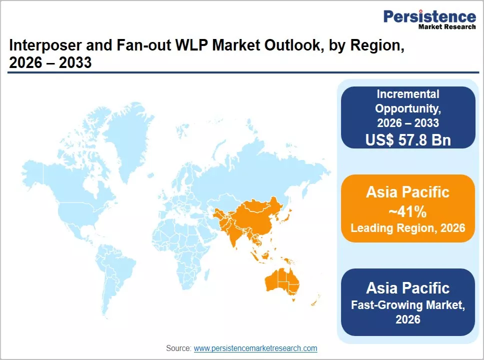
- Leading Region: Asia Pacific is likely to lead the global market with around 41% share in 2026, supported by its extensive semiconductor manufacturing base, established foundries, memory manufacturers, and advanced packaging infrastructure across Taiwan, South Korea, and China.
- Dominant Segment: Fan-out wafer-level packaging is the leading packaging type segment, holding around 54% share in 2026, supported by its ability to deliver thin, compact, and cost-efficient packages for high-volume smartphone, wearable, and power management applications.
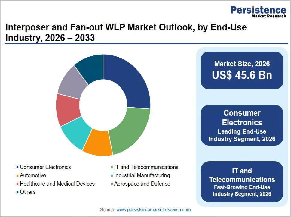
- Fastest-Growing Segment: IT and Telecommunications is the fastest-growing end-use segment, projected to expand at a CAGR of 15.3% from 2026 to 2033, driven by increasing demand for AI servers, data center networks, 5G infrastructure, and advanced semiconductor packaging.
- Key Market Opportunity: Glass and organic interposers present significant growth opportunities by offering potential cost advantages and supporting larger package formats. Early material qualification and manufacturing advancements are expected to help suppliers capture demand as AI chip manufacturers explore alternatives to conventional silicon interposers.
Market Dynamics
Drivers - Surging Demand for AI and High-Performance Computing Chips
Artificial intelligence accelerators and data center processors require extremely high memory bandwidth, making interposer-based packaging increasingly important. An interposer enables processors to connect closely with multiple memory stacks through thousands of high-density electrical connections. This architecture improves data transfer speeds and reduces interconnect distances compared with conventional package designs. As AI models become more computationally intensive, newer chip generations require greater memory bandwidth, additional memory stacks, and more sophisticated packaging architectures, increasing demand for advanced interposer solutions.
High-bandwidth memory from SK hynix, Samsung, and Micron is integrated alongside processors using advanced packaging architectures in several leading AI products. Taiwan Semiconductor Manufacturing Company offers its CoWoS platform to support this integration, and the technology is widely adopted in AI accelerators. Cloud service providers continue investing in data centers and custom AI processors, increasing demand for advanced packaging capacity. Limited availability of qualified packaging capacity has emerged as a supply chain constraint, encouraging manufacturers to expand production lines and invest in specialized equipment.
Growth of Thin, Compact Devices Using Fan-Out Packaging
Consumer demand for slim smartphones, lightweight wearables, and longer battery life is supporting the adoption of fan-out wafer-level packaging. This technology redistributes electrical connections beyond the chip surface, allowing compact package designs without requiring a conventional organic substrate. The architecture reduces package thickness, shortens electrical paths, and supports improved electrical and thermal performance. These advantages are particularly relevant for application processors, power management chips, and radio-frequency components used in space-constrained electronic devices.
Apple adopted Taiwan Semiconductor Manufacturing Company's integrated fan-out process for its A10 processor in 2016, demonstrating the technology's suitability for high-volume consumer electronics production. Outsourced semiconductor assembly and test providers, including ASE Technology, Amkor Technology, and JCET, now offer multiple fan-out packaging solutions. Infineon has also developed embedded wafer-level packaging technologies for applications such as automotive radar and power electronics. Growing adoption of 5G devices and antenna-in-package designs is creating additional demand for compact, high-performance packaging solutions.
Restraints - High Capital Costs and Complex Manufacturing
Advanced semiconductor packaging requires expensive equipment, specialized materials, and controlled manufacturing environments, limiting the number of companies capable of competing at scale. Establishing high-volume interposer or fan-out packaging facilities requires substantial capital investment, while returns depend on securing long-term customer commitments and achieving consistent production yields. Yield losses are particularly costly in advanced packages containing multiple expensive semiconductor dies. A defect in an individual die or interconnection can reduce the overall package yield, increasing manufacturing costs and creating additional challenges for smaller technology providers.
Manufacturing large interposers also presents technical challenges because package dimensions can exceed the exposure limits of conventional lithography equipment, requiring advanced patterning and stitching techniques. Thin wafers are susceptible to warpage during processing, while differences in thermal expansion across materials create additional mechanical stress. Testing and inspection become more complex as multiple dies are integrated into a single package, requiring reliable validation before and after assembly. Heat generated by high-density AI processors further increases thermal management requirements. These manufacturing complexities raise production costs and extend product development cycles.
Limited Advanced Packaging Capacity and Supply Constraints
Demand for advanced semiconductor packaging has periodically exceeded available manufacturing capacity, creating production bottlenecks and delaying product launches. Capacity constraints in advanced interposer packaging affected the supply of AI accelerators during 2023 and 2024. Chip designers often need to secure manufacturing capacity well in advance, while smaller customers face challenges obtaining sufficient production allocations. Extended lead times complicate procurement planning and increase the risk of product redesigns or higher manufacturing costs.
A significant proportion of leading-edge packaging capacity remains concentrated among a limited number of manufacturers, particularly in Taiwan, creating geographic and supply chain concentration risks. Key inputs, including advanced substrates, build-up films, and specialized packaging materials, have also experienced supply constraints. Equipment used for bonding, plating, and inspection can involve extended delivery schedules. Establishing new facilities also requires several years of construction, equipment installation, and customer qualification. Although government initiatives are supporting domestic semiconductor packaging capacity across multiple regions, closing the supply gap remains a gradual process.
Opportunities - Chiplet Designs and Heterogeneous Integration
Semiconductor manufacturers are increasingly adopting chiplet architectures, in which larger monolithic processors are divided into smaller dies that are integrated within a single package. This approach supports improved manufacturing yields, greater design flexibility, and the integration of different semiconductor technologies, including logic, memory, and analog components. Advanced interposers and fan-out redistribution structures provide the high-density electrical connections required to integrate these individual dies. As chiplet adoption expands, advanced packaging is becoming an increasingly important part of semiconductor architecture and product differentiation.
The Universal Chiplet Interconnect Express consortium was established in 2022 to develop an open standard for communication between chiplets. Its membership includes Intel, AMD, Arm, Google, Meta, Microsoft, Qualcomm, Samsung, and Taiwan Semiconductor Manufacturing Company. AMD already uses chiplet architectures in its server and desktop processors. Standardized chiplet interconnects support interoperability between compatible components from different suppliers, creating opportunities for advanced packaging manufacturers, equipment providers, and semiconductor design companies. This development is expected to broaden the adoption of heterogeneous integration across high-performance computing and data center applications.
Glass and Organic Interposers as Lower-Cost Alternatives
Silicon interposers involve relatively high manufacturing costs and face limitations in package dimensions, encouraging semiconductor manufacturers to explore glass and organic alternatives. Glass interposers offer the potential for fine-pitch electrical connections, low signal loss, and larger panel formats, which can improve manufacturing economics. Organic interposers leverage established substrate manufacturing processes and materials, offering potential cost advantages for applications with less demanding interconnect requirements. Suppliers that successfully qualify these alternatives are positioned to benefit as semiconductor manufacturers seek additional packaging materials and greater supply chain flexibility.
Intel announced in September 2023 its plans to introduce glass substrates for advanced packaging in the second half of the decade. Taiwan Semiconductor Manufacturing Company also offers CoWoS variants incorporating organic redistribution structures. Substrate manufacturers such as Ibiden and Unimicron are investing in advanced packaging materials and manufacturing capabilities. Research organizations, including imec and CEA-Leti, continue developing next-generation interposer architectures and packaging technologies, expanding the range of potential solutions available to semiconductor manufacturers.
Category-Wise Analysis
Which Packaging Type Holds the Largest Share of the Market?
Fan-out wafer-level packaging leads the packaging type category with a 54% market share in 2026. It enables compact package designs without requiring a conventional organic substrate, making it suitable for high-volume semiconductor applications. Smartphones, wearables, and power management devices widely use fan-out packaging because of its thin profile, electrical performance, and integration flexibility. The technology has an established manufacturing base, supported by production experience and improvements in process yields. Outsourced semiconductor assembly providers such as ASE Technology, Amkor Technology, and JCET offer fan-out solutions at commercial scale, supporting broader adoption across consumer and industrial electronics.
Interposer packaging is expected to record the fastest growth from 2026 to 2033. AI accelerators, networking chips, and high-performance processors require high-density connections to memory, making interposer-based architectures increasingly important. Growing adoption of high-bandwidth memory and the integration of multiple memory stacks increase requirements for larger and more sophisticated interposers. Cloud service providers are also developing custom AI processors that rely on advanced interconnect technologies. Investments in foundry capacity, advanced packaging equipment, and alternative interposer materials are expected to support faster growth in this segment.
Interposer Material Insights
Silicon represents the leading interposer material category, holding about 68% share of the market in 2026. Silicon supports fine-pitch wiring and through-silicon vias, enabling high-density electrical connections between semiconductor dies and package components. Its thermal expansion characteristics are also compatible with silicon-based semiconductor dies, helping manage mechanical stress during temperature variations. Silicon interposers are commercially established in high-bandwidth memory packages, supported by mature manufacturing processes and proven performance. Taiwan Semiconductor Manufacturing Company uses silicon interposers in its CoWoS-S platform, reinforcing their adoption in advanced AI and high-performance computing applications.
Glass is expected to be the fastest-growing segment from 2026 to 2033. Glass interposers offer the potential for large-format manufacturing, which can improve cost efficiency as package dimensions increase. Their electrical properties, dimensional stability, and smooth surfaces also support fine-pitch circuit formation and high-density interconnections. Major semiconductor manufacturers and materials companies are investing in pilot production lines and specialized manufacturing equipment. Although commercial adoption remains at an early stage, glass interposers offer significant potential as advanced semiconductor packages become larger and more complex.
Packaging Architecture Insights
2.5D packaging leads the packaging architecture category with a 63% share in 2026. This architecture places multiple semiconductor dies side by side on an interposer, enabling high-density connections between processors and memory components. It delivers high memory bandwidth and improved integration while avoiding some of the thermal and manufacturing complexities associated with fully stacked architectures. Xilinx introduced early commercial 2.5D FPGA technology in 2011, and the approach is now widely used in GPUs, networking processors, and high-performance computing applications. Established manufacturing processes and proven design methodologies continue to support its adoption.
3D packaging is expected to record the fastest growth from 2026 to 2033. Vertically stacking semiconductor dies shortens interconnect distances, improves integration density, and supports higher performance within compact package dimensions. Hybrid bonding, which directly connects copper interconnects across semiconductor dies, enables extremely dense electrical connections. AMD uses vertically stacked cache technology in selected Ryzen processors, while Intel offers Foveros and Samsung provides X-Cube packaging technology. Taiwan Semiconductor Manufacturing Company also offers SoIC for advanced die stacking. Increasing demand for AI and server processors with higher performance per watt is expected to accelerate the adoption of 3D packaging.
Which End-Use Industry Leads the Market?
Consumer electronics represents the leading end-use industry, accounting for a 36% share of the market in 2026. Smartphones, tablets, smartwatches, and wireless earbuds require thin, lightweight semiconductor packages, making fan-out packaging suitable for several applications. Frequent consumer electronics product launches generate consistent demand for high-volume semiconductor components. Application processors, power management chips, and radio-frequency components increasingly incorporate advanced packaging technologies. Competitive requirements related to device thickness, battery life, and processing performance encourage electronics manufacturers to adopt advanced packaging solutions.
IT and telecommunications is expected to record the fastest growth from 2026 to 2033. AI servers, data center switches, and 5G network equipment require high-bandwidth memory, advanced processors, and high-density semiconductor interconnections. These applications increasingly rely on interposer-based packaging, chiplet integration, and 3D stacking technologies. Cloud service providers and telecommunications operators continue investing in data center capacity and next-generation network infrastructure. Growing adoption of custom silicon for data center applications is creating additional demand for advanced packages capable of connecting multiple semiconductor dies at high bandwidth.
Regional Analysis
North America Interposer and Fan-Out WLP Market Trends and Insights
North America accounts for an estimated 33% of the global market share in 2026, supported by advanced semiconductor design capabilities and increasing demand for high-performance computing. Leading chip designers, cloud infrastructure providers, and defense contractors are expanding their requirements for advanced semiconductor packaging technologies. The CHIPS and Science Act supports domestic semiconductor manufacturing, packaging research, and supply chain development. Although a substantial share of advanced packaging production remains concentrated in Asia Pacific, regional investments are directed toward expanding domestic manufacturing and packaging capabilities. Growing demand for artificial intelligence processors, chiplet integration, and high-bandwidth memory is expected to support sustained market expansion.
U.S. Interposer and Fan-Out WLP Market Size
The U.S. accounts for 92% of the North American interposer and fan-out WLP market share in 2026, supported by established semiconductor design companies and extensive artificial intelligence infrastructure investments. Leading chip developers, including NVIDIA, AMD, Broadcom, and Intel, increasingly require advanced packaging solutions for high-performance processors. The CHIPS and Science Act encourages domestic packaging research, manufacturing capacity development, and technological innovation. Expanding data center infrastructure also supports demand for high-bandwidth memory integration and advanced interconnect technologies. Growing investments in chiplet architectures, heterogeneous integration, and domestic semiconductor manufacturing are expected to accelerate market growth across the United States.
Europe Interposer and Fan-Out WLP Market Trends and Insights
Europe is projected to hold about 16% share of the interposer and fan-out WLP market in 2026, supported by advanced semiconductor research and established automotive electronics manufacturing. Germany, France, and the Netherlands remain major contributors, driven by industrial semiconductor applications, equipment manufacturing, and packaging technology development. Research organizations, including imec, CEA-Leti, and Fraunhofer institutes, support advancements in chiplet integration and heterogeneous packaging. The European Chips Act encourages domestic semiconductor production and advanced packaging research. Growing investments in automotive electronics, industrial automation, telecommunications equipment, and high-reliability semiconductor packaging are expected to sustain regional market expansion throughout the forecast period.
Germany Interposer and Fan-Out WLP Market Size
Germany accounts for 28% of the European interposer and fan-out WLP market share in 2026, supported by established automotive semiconductor manufacturing and advanced industrial electronics capabilities. Leading technology providers, including Infineon Technologies and Bosch, contribute to demand for advanced semiconductor packaging in automotive radar and power electronics applications. Fraunhofer research institutes support semiconductor packaging development and manufacturing innovation. Increasing adoption of electric vehicles and advanced driver assistance systems is encouraging demand for compact, high-performance semiconductor packages. Growing investments in semiconductor fabrication facilities, heterogeneous integration, automotive electronics, and advanced packaging research are expected to sustain steady market growth across Germany.
France Interposer and Fan-Out WLP Market Size
France represents 16% of the European interposer and fan-out WLP market share in 2026, supported by advanced semiconductor research and established electronics manufacturing capabilities. CEA-Leti contributes to technological development in three-dimensional integration, chiplet architectures, and advanced interconnect solutions. Domestic semiconductor companies, including STMicroelectronics and Soitec, strengthen the country's semiconductor technology ecosystem. Automotive, industrial automation, and aerospace applications generate demand for compact and reliable semiconductor packaging. Growing investments in heterogeneous integration, semiconductor research commercialization, advanced packaging pilot projects, and high-performance electronics are expected to sustain market expansion across France.
Netherlands Interposer and Fan-Out WLP Market Size
The Netherlands is anticipated to hold a 14% share of the European interposer and fan-out WLP market in 2026, supported by an established semiconductor equipment industry and advanced electronics research capabilities. Leading technology providers, including BE Semiconductor Industries, NXP Semiconductors, and ASML, strengthen the domestic semiconductor ecosystem. Increasing adoption of hybrid bonding and three-dimensional chip stacking is creating demand for advanced packaging equipment and assembly technologies. Semiconductor manufacturing equipment, automotive electronics, and precision assembly remain important areas of industry activity. Growing investments in heterogeneous integration, advanced bonding systems, semiconductor research, and next-generation packaging technologies are expected to support market expansion across the Netherlands.
Which Region Leads the Interposer and Fan-Out WLP Market?
Asia Pacific is likely to lead the global interposer and fan-out WLP market, accounting for 41% of revenue share in 2026, supported by extensive semiconductor fabrication and advanced packaging infrastructure. Taiwan, China, and South Korea remain major contributors, driven by established foundries, memory manufacturers, and outsourced semiconductor assembly providers. Strong demand for artificial intelligence processors, smartphones, and high-performance computing supports the adoption of advanced packaging technologies. Regional manufacturers are increasingly investing in interposer production, fan-out wafer-level packaging, and chiplet integration capabilities. Expanding semiconductor manufacturing capacity, technological advancements, and integrated supply chains are expected to sustain Asia Pacific's market leadership through 2033.
China Interposer and Fan-Out WLP Market Size
China accounts for 24% of the Asia Pacific interposer and fan-out WLP market share in 2026, supported by expanding semiconductor manufacturing and domestic advanced packaging capabilities. Leading assembly providers, including JCET and Tongfu Microelectronics, contribute to fan-out packaging development and heterogeneous integration. Government initiatives supporting semiconductor localization encourage investment in domestic packaging facilities and advanced manufacturing equipment. Increasing demand for artificial intelligence processors and consumer electronics is strengthening requirements for advanced packaging solutions. Growing investments in chiplet integration, advanced interconnect technologies, semiconductor self-sufficiency, and domestic manufacturing capacity are expected to sustain market expansion across China's semiconductor industry.
Taiwan Interposer and Fan-Out WLP Market Size
Taiwan is expected to hold about 33% share of the Asia Pacific interposer and fan-out WLP market in 2026, supported by extensive semiconductor foundry operations and advanced packaging manufacturing capabilities. Taiwan Semiconductor Manufacturing Company leads technological development in CoWoS and integrated fan-out packaging, while ASE Technology contributes significantly to outsourced semiconductor assembly and packaging services. Growing demand for artificial intelligence accelerators and high-performance computing processors is supporting advanced packaging capacity expansion. Strong integration between semiconductor fabrication and packaging operations strengthens Taiwan's competitive position. Increasing investments in chiplet integration, high-bandwidth memory packaging, and next-generation interconnect technologies are expected to sustain its market leadership.
South Korea Interposer and Fan-Out WLP Market Size
South Korea is anticipated to account for 17% of the Asia Pacific interposer and fan-out WLP market share in 2026, supported by advanced memory manufacturing and semiconductor packaging capabilities. Leading manufacturers, including SK hynix and Samsung, contribute to high-bandwidth memory development and advanced chip integration technologies. Increasing demand for artificial intelligence processors is encouraging the adoption of interposer-based packaging and three-dimensional semiconductor stacking. Domestic manufacturers are also investing in advanced packaging platforms, including Samsung's I-Cube and X-Cube technologies. Growing investments in memory integration, heterogeneous packaging, semiconductor manufacturing modernization, and high-performance computing applications are expected to accelerate market expansion across South Korea.
Competitive Landscape
The global interposer and fan-out WLP market is moderately consolidated, with established semiconductor foundries and outsourced assembly providers controlling advanced packaging capacity. Competition focuses on manufacturing scale, packaging reliability, production yields, and technological capabilities. Leading manufacturers benefit from substantial capital investments, established customer relationships, and advanced integration technologies. Interposer packaging, fan-out wafer-level packaging, and heterogeneous integration remain major areas of product differentiation.
Market participants increasingly invest in capacity expansion, advanced materials, and collaborative chip development. Emerging companies target glass substrates, panel-level fan-out packaging, and inspection technologies. Supply chain partnerships, equipment innovation, and specialized packaging solutions strengthen competitive positioning.
Key Industry Developments
- In September 2024, SK hynix began mass production of 12-layer HBM3E memory products, which pair with interposers in AI accelerators and increase demand for advanced packaging capacity and for high-density interconnect designs.
- In December 2024, Amkor Technology received a preliminary CHIPS Act funding award of about US$ 400 million to support an advanced packaging facility in Arizona, adding local capacity for AI and high-performance chips in the United States.
- In December 2024, SKC’s subsidiary Absolics received a preliminary CHIPS Act award to support its glass substrate plant in Georgia, advancing glass as a new material for advanced chip packaging in the United States.
Companies Covered in Interposer and Fan-out WLP Market
- Taiwan Semiconductor Manufacturing Company Limited (TSMC)
- Samsung Electronics Co., Ltd.
- Intel Corporation
- ASE Technology Holding Co., Ltd.
- Amkor Technology, Inc.
- JCET Group Co., Ltd.
- Powertech Technology Inc.
- United Microelectronics Corporation
- GlobalFoundries Inc.
- Nepes Corporation
- Siliconware Precision Industries Co., Ltd.
- ChipMOS Technologies Inc.
- Tongfu Microelectronics Co., Ltd.
- Unimicron Technology Corporation
- AT&S Austria Technologie & Systemtechnik AG
Frequently Asked Questions
The global interposer and fan-out WLP market size is estimated at US$ 45.6 billion in 2026 and is projected to reach US$ 103.4 billion by 2033, growing at a CAGR of 12.4% between 2026 and 2033.
Demand is driven by increasing adoption of AI and high-performance computing chips that require higher memory bandwidth, along with growing demand for thin, compact consumer electronics using fan-out packaging. Integration of high-bandwidth memory alongside processors through interposer-based packaging further increases demand for advanced packaging solutions and raises the value per package.
Asia Pacific is likely to lead the global market with a 41% share in 2026, supported by its established semiconductor manufacturing ecosystem across Taiwan, South Korea, and China. The region hosts major foundries, memory manufacturers, and outsourced semiconductor assembly providers.
Chiplet integration and the development of lower-cost glass and organic interposers present key market opportunities. Growing interest in alternative interposer materials also creates opportunities to reduce packaging costs and support larger semiconductor packages.
Key players in the market include Taiwan Semiconductor Manufacturing Company, ASE Technology, Amkor Technology, JCET, and Samsung Electronics.


