


- Semiconductor Materials & Components
- Semiconductor Metrology and Inspection Equipment Market
Semiconductor Metrology and Inspection Equipment Market Size, Share, and Growth Forecast 2026 - 2033
Semiconductor Metrology and Inspection Equipment Market by Technology (Inspection Equipment, Metrology Equipment), Dimension (2D, 3D Metrology/Inspection), Process Node (≤ 7 nm, 8-14 nm), Fab Type (Foundry, Memory), and Regional Analysis, 2026 - 2033
Semiconductor Metrology and Inspection Equipment Market Size and Trends Analysis
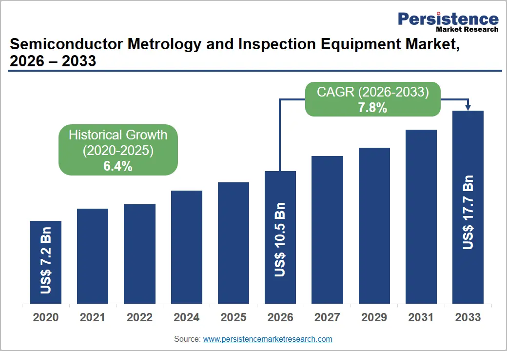
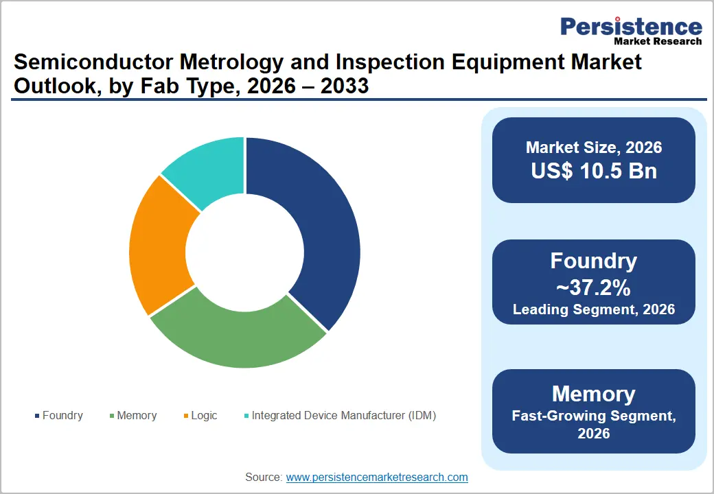
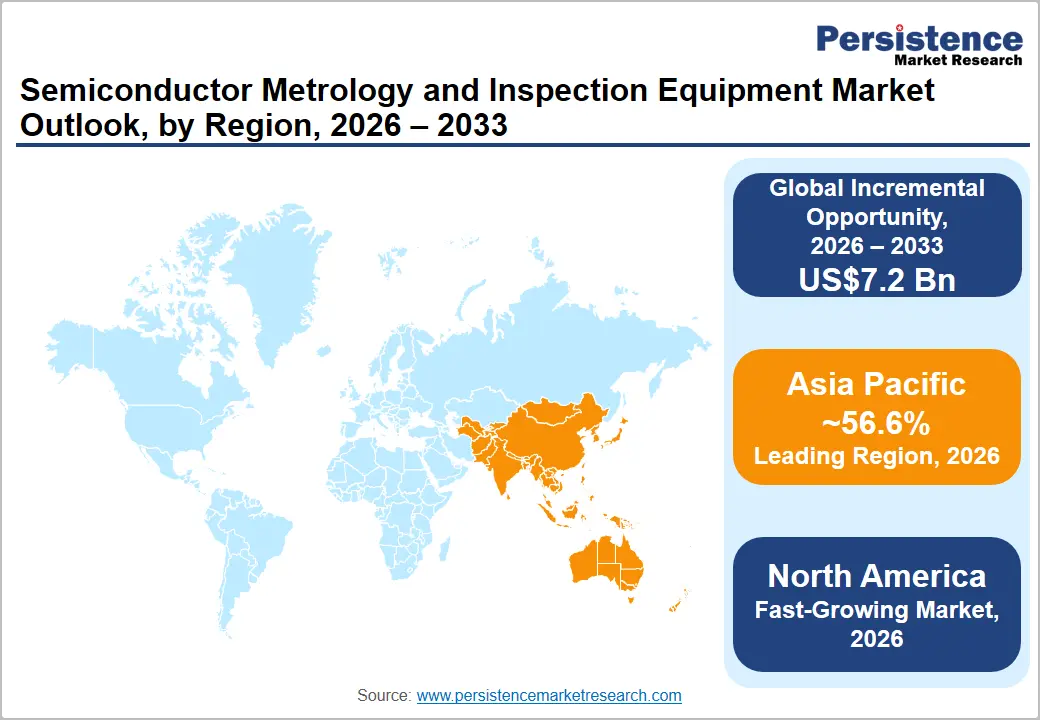
The global semiconductor metrology and inspection equipment market size is likely to be valued at US$10.5 billion in 2026 and is estimated to reach US$17.7 billion by 2033, growing at a CAGR of 7.8% during the forecast period from 2026 to 2033, driven by increasing adoption of sub-5nm and 3nm process nodes, which require advanced defect detection and precise measurement capabilities. Increasing use of EUV and High-NA lithography is further fostering demand for high-resolution inspection and metrology tools.
Key Industry Highlights:
- New Study: In April 2026, researchers introduced SemiFA, an AI-based framework for autonomous semiconductor failure analysis. The system integrates inspection images, equipment telemetry, historical defect records, and multimodal AI models to generate structured failure analysis reports in less than one minute.
- Leading Region: Asia Pacific, with about 56.6% share in 2026, owing to its superior concentration of high-volume semiconductor manufacturing hubs.
- Fastest-growing Region: North America, backed by large-scale fab investments supported by the U.S. Department of Commerce.
- Leading Technology: Inspection equipment, approximately 58.4% share in 2026, as it enables early-stage defect detection across multiple process steps.
- Dominant Fab Type: Foundry, nearly 37.2% share in 2026, as companies such as TSMC manufacture chips for multiple fabless firms.
DRO Analysis
Driver - Advanced Node Manufacturing to Push Optical Inspection to Its Physical Limits
At sub-7 nanometer (nm) process nodes, conventional optical inspection tools begin losing sensitivity to the defects that matter most. Gate-All-Around (GAA) transistors, now entering high-volume manufacturing at leading foundries, require Critical Dimension (CD) measurement precision of 0.5 nm or better. Any deviation beyond that threshold can compromise transistor switching behavior and chip performance.
According to the 2024 International Roadmap for Devices and Systems (IRDS) Metrology report published by the Institute of Electrical and Electronics Engineers (IEEE), the transition to High Numerical Aperture (High-NA) Extreme Ultraviolet (EUV) lithography is creating new challenges. This technology uses a numerical aperture of 0.55. It is anticipated to enter high-volume manufacturing between 2025 and 2026. At this level, new stochastic defect patterns and pattern variability emerge, which are difficult to predict and control. This has surged demand for hybrid Electron Beam (e-beam) and X-ray metrology platforms.
Deep Memory Architectures to Require Subsurface Inspection Capabilities
The vertical expansion of 3D NAND flash memory beyond 200 layers has created a category of measurement problems that standard metrology tools were not designed to solve. As layer counts increase, channel hole etching becomes deeper, aspect ratios rise, and critical defects move further below the wafer surface, out of reach of Optical Critical Dimension (OCD) and Critical Dimension Scanning Electron Microscopy (CD-SEM) tools.
According to the 2025 SPIE Metrology, Inspection, and Process Control XXXIX proceedings, 3D NAND multilayer stacks present unique challenges across vertical gate control, channel hole Critical Dimension (CD), and material characterization, with no single metrology technique providing a complete solution. Once 3D NAND crosses the 200-layer threshold, traditional methods start to break down, as dense material stacks and deep trench structures make it difficult to measure critical dimensions at the bottom of features. This has made subsurface metrology tools a mandatory investment category for memory fabs.
Restraint - Steep Price of High-Resolution Inspection Tools
Electron Beam (e-beam) and Extreme Ultraviolet (EUV) mask inspection tools provide unmatched defect sensitivity. However, their cost remains prohibitive for all but the most advanced fabrication facilities. High installation costs remain a significant barrier, especially for small manufacturers. Getinge AB's 2024 launch of a next-generation isolator with automated bio-decontamination reflects the industry's move toward advanced contamination control solutions. E-beam systems in particular carry a further throughput penalty.
They are substantially slower than optical tools, which means deploying them across a high-volume fab requires either a large number of units or selective use on critical layers only. In its 2024 investor day presentation filed with the U.S. Securities and Exchange Commission (SEC), ASML acknowledged that the Total Addressable Market (TAM) for its holistic metrology and inspection business is anticipated to rise from €5.4 billion (nearly US$6.1 billion) in 2023 to €11 billion (around US$12.6 billion) by 2030. This shows the intensity of the demand, but also the fact that only the well-capitalized fabs can afford the full tool stack today.
Opportunity - On-Tool AI to Reduce Yield Loss from Undetected Process Drift
Embedding Artificial Intelligence (AI) and Machine Learning (ML) into metrology and inspection tools is changing how fabs detect and respond to process excursions. Rather than flagging defects after the fact, AI-enabled tools can identify spatial signatures and predict process drift before it causes yield-impacting failures. KLA Corporation, which holds approximately 50% of the process control equipment market, has integrated deep learning into its inspection platforms to distinguish true defect signals from pattern noise.
Its Klarity Defect software connects data across multiple tool types to deliver automated yield root cause analysis. AI classification has been shown to reduce recipe setup time by 20%, improving fab throughput. In February 2025, Applied Materials introduced its SEMVision H20 defect review system, which combines sensitive e-beam imaging with AI-backed image recognition for rapid analysis of buried nanoscale defects. It targets the latency between detection and corrective action.
Surface Measurement Tools to Become Central to Chiplet-Era Packaging
Hybrid bonding, a technique that joins two semiconductor surfaces without adhesive layers, is now a key process in advanced chiplet and memory packaging. It demands angstrom-level surface preparation across copper contact pads and dielectric layers. If surface roughness, dishing, or contamination falls outside specification, bonding integrity is compromised, and the entire stacked assembly fails.
According to a 2025 application note from Bruker Corporation, successful hybrid bonding requires pristine surface conditions regardless of the method, with critical metrics such as defectivity, surface roughness, and copper contact pad recess depth, all of which must be tightly controlled. Research presented at the 2024 SPIE Advanced Lithography and Patterning conference by engineers from Micron Technology and KLA Corp confirmed that advanced overlay metrology and process control are essential for achieving reliable wafer-to-wafer hybrid bonding at volume. This helps in establishing bonding metrology as a growth segment in its own right.
Category-wise Analysis
Technology Insights
The inspection equipment segment is expected to lead with a share of approximately 58.4% in 2026, as it helps detect defects early and at multiple stages of semiconductor manufacturing. Modern chips have billions of transistors, and even a tiny defect can cause failure. Optical and e-beam inspection tools can scan wafers layer by layer and identify defects before they propagate. This reduces yield loss in later stages, which are far more expensive to fix. Another driver is the adoption of EUV lithography.
EUV introduces stochastic defects that are random and hard to predict. A 2024 EUV defect study by IMEC showed that stochastic defects can affect line edge roughness and device reliability. Inspection tools are the only way to identify these random defects in real time.
The metrology equipment segment is estimated to be the fastest-growing over the forecast period, as it provides precise measurement of critical dimensions and process parameters. The need for metrology has increased due to complex device architectures such as gate-all-around (GAA) transistors and 3D NAND. These structures require measurement of vertical and buried features. According to the National Institute of Standards and Technology, advanced nodes require sub-nanometer measurement accuracy. This level of precision is only possible with advanced metrology tools such as scatterometry and CD-SEM.
Fab Type Insights
Foundry is anticipated to dominate with a share of nearly 37.2% in 2026, as they serve multiple customers across industries. Companies such as TSMC and Samsung Electronics manufacture chips for firms that do not own fabs, including Apple, NVIDIA, and Qualcomm. This model allows high utilization of expensive fabrication facilities. The fabless trend has fueled in the past decade. According to reports from the Semiconductor Industry Association, multiple chip designers prefer outsourcing manufacturing to reduce capital expenditure and focus on design innovation. This has increased demand for foundry services.
The memory segment is expected to remain in the second position in 2026, owing to rising data demand from AI, cloud, and edge computing. Applications such as generative AI require large amounts of High-Bandwidth Memory (HBM) and Dynamic Random Access Memory (DRAM). This has increased investment in memory manufacturing. Companies such as SK Hynix and Micron Technology are broadening capacity for HBM. In 2024, SK Hynix announced mass production of HBM3E, which is used in AI accelerators. This shows how memory demand is associated with AI growth.
Regional Insights
Asia Pacific Semiconductor Metrology and Inspection Equipment Market Trends
Asia Pacific is anticipated to lead in 2026 with a share of nearly 56.6%, as it hosts the largest concentration of semiconductor manufacturing hubs. Taiwan, South Korea, China, and Japan account for most global wafer production. Foundries such as TSMC and memory leaders, including Samsung Electronics, operate at a very large scale. This creates continuous demand for inspection and metrology tools. Governments in the region actively support the market. For example, South Korea announced a national semiconductor cluster plan backed by policy support and infrastructure investment. Japan is also funding advanced fabs and materials supply chains. These policies ensure steady equipment demand.
China Semiconductor Metrology and Inspection Equipment Market Trends
China will likely lead in Asia Pacific in 2026 with a share of around 40.4%, backed by its push for semiconductor self-sufficiency. The government has introduced large funding programs under the Made in China strategy. According to releases from the Ministry of Industry and Information Technology of China, the country is increasing investments in domestic chip manufacturing and equipment. Local foundries such as SMIC are broadening capacity. Despite export restrictions, SMIC has reported progress in advanced-node production using domestic tools. This has increased demand for local inspection and metrology systems.
India Semiconductor Metrology and Inspection Equipment Market Trends
In 2026, India is projected to account for a share of approximately 27.8%, as the country is at an early stage but shows policy-driven growth. The government has launched semiconductor incentive schemes to attract global players. The Ministry of Electronics and Information Technology has approved multiple semiconductor and OSAT projects. One key development is the approval of fabrication and packaging units involving companies such as Micron Technology. Micron is setting up a semiconductor assembly and test facility in Gujarat. This marks a shift from design-only presence to manufacturing.
North America Semiconductor Metrology and Inspection Equipment Market Trends
North America is predicted to be the fastest-growing market in 2026 with a share of approximately 24.7%, fueled by government-backed reshoring efforts. The U.S. Department of Commerce is implementing the CHIPS and Science Act to boost domestic manufacturing. This includes funding for new fabs and equipment. Dominant companies are building new facilities. Intel is broadening fabs in Arizona and Ohio. TSMC is also constructing advanced fabs in the U.S. These projects are increasing demand for inspection and metrology tools.
U.S. Semiconductor Metrology and Inspection Equipment Market Trends
A share of nearly 59.3% is expected to be held by the U.S. in 2026, supported by large-scale investments and policy support. The CHIPS Act has triggered multiple fab announcements across states such as Arizona, Texas, and New York. Companies, including Intel and GlobalFoundries, are extending capacity. Intel’s roadmap includes advanced-node manufacturing, which requires high-end inspection tools. The U.S. also leads in semiconductor equipment and software. Firms such as KLA Corporation and Applied Materials are global leaders in process control, which gives the country a superior position across the value chain.
Europe Semiconductor Metrology and Inspection Equipment Market Trends
Europe will likely see decent growth over the forecast period with a share of nearly 15.8% in 2026, propelled by focused investments and niche strengths. The European Commission has introduced the European Chips Act to extend semiconductor capacity. Europe is dominant in equipment and materials rather than large-scale fabs. Companies such as ASML lead EUV lithography. This creates consistent demand for metrology and inspection tools associated with advanced lithography. The region is further investing in automotive and industrial chips. These segments require reliable and mature-node manufacturing, which supports stable equipment demand.
Germany Semiconductor Metrology and Inspection Equipment Market Trends
Germany will likely register a substantial share of approximately 35.4% in 2026, owing to its well-established industrial base and automotive sector. Automotive companies require advanced chips for electric vehicles and autonomous systems. This propels semiconductor demand. Germany is attracting key investments. Intel has announced plans for a large fab project in Magdeburg. Infineon Technologies is also extending power semiconductor production. Government support is rising steadily. Authorities are providing subsidies for semiconductor projects under EU initiatives, which is improving local manufacturing capacity.
U.K. Semiconductor Metrology and Inspection Equipment Market Trends
A share of around 16.5% is predicted to be held by the U.K. in 2026, as companies are focusing on design, research, and niche technologies rather than large-scale fabrication. The government has released a national semiconductor strategy to support innovation and supply chain resilience. The U.K. has strengths in chip design and IP development. Companies such as Arm Ltd. play a global role in processor architecture, which keeps the country relevant in the semiconductor industry.
Competitive Landscape
The global semiconductor metrology and inspection equipment market is highly consolidated and oligopolistic with a handful of technology-intensive companies controlling most of the industry. KLA Corporation remains the undisputed leader in the market, especially in wafer inspection and process control. Industry estimates suggest that KLA controls more than half of the global inspection and metrology segment and maintains dominant positions in optical inspection and reticle inspection systems.
A second tier of competitors includes Onto Innovation, Nova, Camtek, Lasertec, SCREEN Semiconductor Solutions, and Thermo Fisher Scientific. These companies focus on specialized segments such as advanced packaging, compound semiconductors, hybrid metrology, EUV mask inspection, and nanoscale failure analysis. Competition is shifting from hardware performance alone to AI-based defect classification, software analytics, hybrid metrology, and process-control networks.
Key Industry Developments:
- In April 2026, Camtek signed a definitive agreement to acquire Visual Layer, an AI company specializing in visual analytics. Camtek stated that Visual Layer’s proprietary AI technologies would improve its semiconductor inspection and metrology offerings by improving automated defect detection, classification, and visual analysis capabilities.
- In March 2026, Onto Innovation launched the Dragonfly G5 inspection platform for semiconductor manufacturing. The new system was designed for sub-micron defect detection in high-volume manufacturing environments. The platform supports advanced packaging applications and next-generation semiconductor devices that require high inspection sensitivity.
- In February 2026, Siemens announced the acquisition of Canopus AI to extend its semiconductor metrology and inspection software capabilities. Siemens stated that the acquisition would strengthen its semiconductor manufacturing software portfolio by integrating advanced AI-based metrology solutions.
Companies Covered in Semiconductor Metrology and Inspection Equipment Market
- Applied Materials, Inc.
- ASML
- Camtek
- Hitachi High-Tech Corporation
- KLA Corporation
- Lasertec Corporation
- Nova Ltd.
- Onto Innovation
- SCREEN Semiconductor Solutions Co., Ltd.
- Thermo Fisher Scientific Inc.
- Others
Frequently Asked Questions
The global semiconductor metrology and inspection equipment market is projected to be valued at US$10.5 billion in 2026.
The semiconductor metrology and inspection equipment market is expected to reach US$17.7 billion by 2033.
Key market trends include rising adoption of AI-enabled inspection systems and increasing demand for hybrid metrology.
Inspection equipment is expected to be the leading technology with a share of nearly 58.4% in 2026, owing to its ability to support AI-assisted defect classification.
The semiconductor metrology and inspection equipment market is expected to grow at a CAGR of 7.8% from 2026 to 2033.
Applied Materials, Inc., ASML, and Camtek are a few key market players.


