


- Specialty & Fine Chemicals
- Wet Process Equipment Market
Wet Process Equipment Market Size, Share, and Growth Forecast, 2026 - 2033
Wet Process Equipment Market by Product Type (Cleaning Systems, Etching Systems, Others), Equipment Type (Automatic, Semi-automatic, Others), Application, and Regional Analysis for 2026 - 2033
Wet Process Equipment Market Size and Trends Analysis
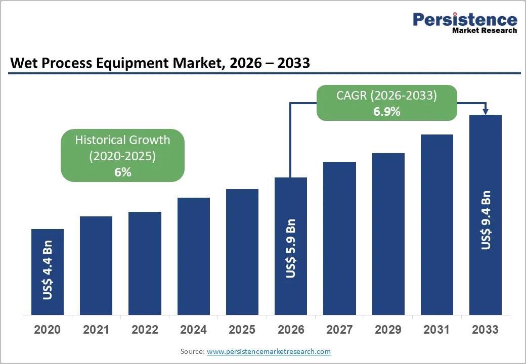
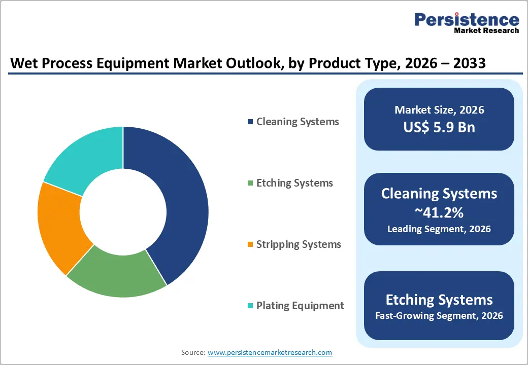
The global wet process equipment market size is likely to be valued at US$5.9 billion in 2026 and is expected to reach US$9.4 billion by 2033, growing at a CAGR of 6.9% between 2026 and 2033, driven by advanced-node semiconductor manufacturing, increasing adoption of advanced packaging technologies, and stricter contamination-control requirements across fabrication processes.
Global supply chain localization policies and the transition toward high-precision cleaning, etching, stripping, and plating processes in logic, memory, MEMS, and power semiconductor production further reinforce demand. The market reflects long-term industrial demand rather than cyclical spikes.
Key Industry Highlights:
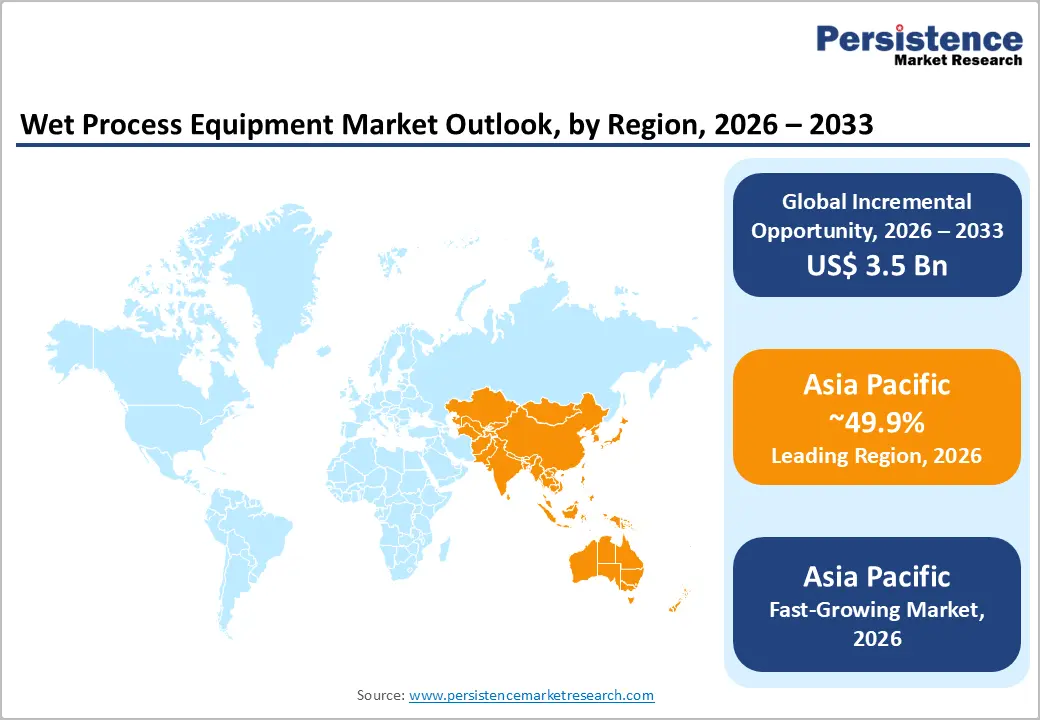
- Leading Region: Asia Pacific is projected to account for approximately 49.9% of market share, driven by high semiconductor manufacturing concentration and strong supply chain ecosystems.
- Fastest-growing Region: Asia Pacific is also the fastest-growing, supported by expanding semiconductor investments in China, India, and Southeast Asia, as well as increasing adoption of advanced packaging technologies.
- Investment Plans: Global semiconductor investments, supported by policy initiatives such as the CHIPS Act and similar programs, are driving multi-billion-dollar fab expansions, significantly increasing demand for wet process equipment across North America, Europe, and Asia.
- Dominant Product Type: Cleaning systems are anticipated to lead, with a global share of over 41.2%, due to their critical role in contamination control and yield optimization.
- Leading Equipment Type: Automatic equipment dominates, accounting for 57.8% of the market, driven by the need for high precision, throughput, and process consistency in semiconductor manufacturing.
| Key Insights | Details |
|---|---|
| Wet Process Equipment Market Size (2026E) | US$5.9 Bn |
| Market Value Forecast (2033F) | US$9.4 Bn |
| Projected Growth (CAGR 2026 to 2033) | 6.9% |
| Historical Market Growth (CAGR 2020 to 2025) | 6.0% |
DRO Analysis
Driver Analysis - AI, HPC, and Advanced Packaging Increasing Process Complexity
The rapid expansion of artificial intelligence (AI), high-performance computing (HPC), and advanced packaging technologies is significantly increasing the number and complexity of wet processing steps. Advanced semiconductor nodes require finer geometries, higher interconnect density, and multi-layer architectures, all of which demand more frequent cleaning, etching, and stripping processes.
The growth of AI-driven data centers is accelerating semiconductor demand, particularly for high-bandwidth memory (HBM) and advanced logic chips. These technologies require wafer backside processing, hybrid bonding, and ultra-clean surfaces, thereby increasing reliance on wet-process equipment. As a result, manufacturers are adopting single-wafer processing systems and higher levels of automation to optimize yield and reduce defects.
Government-Led Semiconductor Localization Initiatives
Government policies aimed at strengthening domestic semiconductor manufacturing capabilities are driving substantial investment in fabrication facilities. Incentive programs across North America, Europe, and Asia are encouraging the construction of new fabs and the expansion of existing facilities. Public funding initiatives are supporting capital expenditure for semiconductor manufacturing infrastructure, research, and workforce development.
These policies are creating a favorable environment for equipment suppliers, including wet process equipment manufacturers, by increasing demand for front-end and back-end processing tools. The construction of multiple new fabrication plants globally is expected to sustain equipment demand over the forecast period. This structural shift toward localized production reduces supply chain risks and enhances long-term market stability.
Expansion of MEMS and Energy-Related Applications
Wet process equipment demand is expanding beyond traditional semiconductor applications into MEMS devices and energy-related manufacturing, including solar photovoltaics. MEMS devices require high-precision microfabrication processes, which rely heavily on wet etching and cleaning techniques.
The growth of renewable energy infrastructure, particularly solar PV, is driving demand for wafer-processing technologies used in cell manufacturing. Wet processing plays a critical role in surface treatment, texturing, and material refinement. This diversification of application areas is broadening the addressable market and reducing dependence on a single end-use segment, thereby enhancing overall market resilience.
Restraint Analysis - High Operating Costs and Resource Intensity
Wet-process equipment incurs high operating costs due to significant chemical and ultrapure water (UPW) consumption. Maintaining consistent chemical composition, temperature, and contamination levels requires advanced process control systems and continuous monitoring. Water usage is particularly critical, as semiconductor fabrication demands extremely high-quality water. Any disruption in supply or quality can directly impact yield and operational efficiency. These factors increase the total cost of ownership, especially for smaller manufacturers and facilities in resource-constrained regions.
Environmental Regulations and Sustainability Pressures
Stringent environmental regulations governing chemical usage, wastewater treatment, and emissions are creating compliance challenges for manufacturers. Wet processing generates chemical waste that must be treated and disposed of in accordance with regulatory standards. Increasing focus on sustainability is pushing companies to adopt eco-friendly chemistries and reduce water consumption. While this creates innovation opportunities, it also raises capital and operational expenditures. Compliance requirements can slow down equipment adoption, particularly in cost-sensitive markets.
Opportunity Analysis - Growth in Emerging Semiconductor Markets
Emerging economies such as India and Southeast Asian countries are becoming key destinations for semiconductor manufacturing investments. Government incentives and industrial policies are encouraging the development of local semiconductor ecosystems. These markets often require cost-effective and scalable equipment solutions, creating opportunities for semi-automated and modular wet process systems. Vendors that can provide flexible and affordable solutions are well-positioned to capture market share in these regions.
Technological Advancements in Single-Wafer Processing
The shift from batch processing to single-wafer processing is creating opportunities for equipment manufacturers to develop high-precision, low-defect solutions. Single-wafer systems offer better process control, uniformity, and reduced chemical consumption. Advancements in automation, real-time monitoring, and process integration are enabling manufacturers to improve throughput while maintaining high quality. These innovations are particularly relevant for advanced-node semiconductor manufacturing and advanced packaging applications.
Sustainability-Driven Innovation in Wet Processing
The increasing emphasis on sustainability is driving innovation in chemical recycling, water reuse, and eco-friendly process chemistries. Equipment manufacturers are developing solutions that minimize environmental impact while maintaining performance. Technologies that reduce chemical consumption, improve waste treatment efficiency, and enable closed-loop systems are gaining traction. Companies that invest in sustainable solutions can differentiate themselves and meet evolving regulatory and customer requirements.
Category-wise Analysis
Product Type Insights
Cleaning systems are expected to dominate, maintaining a leading share of 41.2% in 2026. This dominance is driven by the critical role of contamination control in semiconductor manufacturing. As device geometries continue to shrink below advanced nodes, even nanoscale particles can significantly impact yield, making cleaning processes indispensable across all fabrication stages.
Cleaning systems are extensively used in both front-end (FEOL) and back-end (BEOL) processes, ensuring effective surface preparation, residue removal, and particle control. For example, single-wafer cleaning platforms used in advanced logic fabs are critical for removing post-etch residues and preventing cross-contamination in multi-patterning processes. Their importance is further amplified in advanced packaging technologies such as 2.5D/3D ICs, where surface integrity directly influences interconnect reliability and bonding performance.
Etching systems are expected to be the fastest-growing segment, driven by increasing demand for precise material removal in advanced semiconductor nodes. High-aspect-ratio structures, complex device architectures, and emerging materials such as silicon carbide (SiC) and gallium nitride (GaN) require highly controlled and selective etching processes.
The growth of AI, 5G, and advanced packaging technologies is accelerating demand for etching systems that deliver high uniformity and minimal substrate damage. For instance, wet etching processes are widely used in power semiconductor manufacturing for SiC wafers and in advanced packaging for redistribution layer (RDL) formation. While stripping systems and plating equipment remain essential for resist removal and metallization, etching systems are experiencing the most rapid growth due to their critical role in enabling next-generation device architectures.
Equipment Type Insights
Automatic equipment is expected to lead the market, holding around 57.8% of the market share in 2026. This leadership is driven by the need for high throughput, precision, and repeatability in semiconductor fabrication. Automated systems significantly reduce human intervention, minimizing contamination risks and ensuring consistent process outcomes. These systems are widely deployed in high-volume semiconductor fabs where yield optimization and operational efficiency are critical.
For example, fully automated wet benches integrated with robotic wafer handling systems are commonly used in 300mm fabs to maintain cleanroom standards and ensure uniform chemical processing. Automation also enables real-time monitoring of process parameters, such as chemical concentration and temperature, thereby improving performance and sustainability.
Semi-automatic equipment is expected to be the fastest-growing segment, particularly in emerging markets and research-oriented environments. These systems provide a balance between cost efficiency and operational control, making them suitable for pilot production, academic research, and specialty device manufacturing.
Semi-automatic systems are increasingly adopted in MEMS fabrication facilities and compound semiconductor production, where batch sizes are smaller and process flexibility is essential. For instance, research labs and startups developing MEMS sensors or GaN-based devices often rely on semi-automated wet benches due to their lower capital requirements and adaptability. As semiconductor ecosystems expand in emerging economies, demand for these cost-effective and scalable solutions is expected to rise steadily.
Regional Insights
North America Wet Process Equipment Market Trends - CHIPS Act-Driven Fab Expansion and Sustainable Process Innovation
North America represents a significant market for wet process equipment, driven by strong semiconductor manufacturing capabilities and a robust innovation ecosystem. The U.S. leads the region, supported by substantial government funding and policy initiatives aimed at strengthening domestic semiconductor production. The implementation of the CHIPS and Science Act has accelerated investments in new fabrication facilities, including projects by Intel in Ohio and TSMC in Arizona. These fabs require advanced wet cleaning, etching, and plating systems, directly increasing demand for high-precision equipment.
The region benefits from the presence of major semiconductor equipment manufacturers such as Applied Materials and Lam Research, both of which have expanded their portfolios in single-wafer cleaning and advanced packaging solutions. For example, Lam Research has continued to invest in wafer cleaning technologies tailored for advanced nodes and 3D device architectures, reinforcing North America’s position in high-end equipment innovation. At the same time, IBM Research has collaborated with ClassOne Technology on next-generation solvent processing, highlighting the role of R&D partnerships in driving sustainable wet processing advancements.
Regulatory focus on environmental sustainability and resource efficiency is influencing equipment design and adoption. Companies are investing in technologies that reduce water and chemical usage while maintaining high performance. For instance, equipment suppliers are integrating chemical recycling and ultrapure water optimization systems into their platforms to comply with tightening environmental standards. The region continues to attract investment in new fabrication facilities, and these developments are reinforcing demand for automated, high-throughput wet process systems.
Europe Wet Process Equipment Market Trends - Chips Act Support and Precision Engineering with Sustainability Focus
Europe is an important market characterized by strong policy support and technological expertise. The European Chips Act is driving investments aimed at enhancing semiconductor self-sufficiency, encouraging both domestic manufacturing and foreign direct investment. This policy framework has supported major projects such as Intel’s planned fab expansion in Germany, which is expected to increase demand for wet processing equipment across front-end and advanced packaging applications.
Germany, France, and the U.K. are key contributors to the regional market. Germany serves as a hub for equipment manufacturing and engineering, with companies such as RENA Technologies and AP&S International actively developing advanced wet benches and single-wafer platforms. RENA Technologies’ launch of automated wet processing systems for 200mm and 300mm wafers reflects Europe’s focus on precision engineering and process optimization.
France contributes through industrial and chemical expertise, with Technic Inc. maintaining manufacturing and R&D operations that support electroplating and surface treatment solutions used in semiconductor fabrication. The U.K. continues to play a role in research and innovation, particularly in compound semiconductors and photonics, which rely on specialized wet processing techniques.
The region’s regulatory environment emphasizes sustainability and environmental compliance, encouraging the adoption of eco-friendly technologies. European manufacturers are increasingly investing in low-chemical-consumption systems and closed-loop water recycling solutions to meet stringent environmental standards. While Europe has a smaller manufacturing base compared to Asia, ongoing investments and policy support are expected to drive steady growth, particularly in high-value and specialized applications.
Asia Pacific Wet Process Equipment Market Trends - Fab Concentration and Advanced Node Manufacturing Dominance
Asia Pacific is projected to dominate the market, accounting for approximately 49.9% of market share in 2026. The region’s leadership is driven by the concentration of semiconductor manufacturing facilities, strong supply chain networks, and extensive government support.
China, Taiwan, South Korea, and Japan are major contributors, with extensive fabrication capacity and ongoing investments in advanced technologies. For example, TSMC continues to expand its advanced-node manufacturing capacity, which directly increases demand for high-precision wet cleaning and etching systems. Samsung Electronics is also investing in advanced memory and logic fabs, requiring sophisticated wet processing solutions for high-density device architectures.
Japan remains a critical equipment and technology provider, with companies such as SCREEN Holdings and Tokyo Electron leading in cleaning and coater/developer technologies. SCREEN Holdings, for instance, continues to supply advanced wafer cleaning systems to global fabs, reinforcing the region’s technological leadership in wet processing.
China’s semiconductor expansion, supported by state-backed initiatives, is increasing domestic demand for wet process equipment, particularly in mature-node and power semiconductor manufacturing. India is also emerging as a strategic growth market, with investments by Tata Electronics and government-backed semiconductor programs driving the development of local fabrication capabilities.
Key growth drivers include high manufacturing density, advanced packaging capabilities, and favorable industrial policies. The region benefits from well-established supplier ecosystems across Taiwan, Japan, South Korea, and China, enabling faster adoption of new technologies and shorter equipment qualification cycles. These developments collectively reinforce Asia Pacific’s dominance and position it as the primary growth engine for the wet process equipment market.
Competitive Landscape
The global wet process equipment market exhibits a moderately fragmented structure, with a mix of large multinational corporations and specialized niche players. Leading companies dominate high-end applications and integrated solutions, while smaller firms focus on specific technologies such as cleaning, etching, and plating.
Market competition is driven by technological innovation, process expertise, and customer relationships. Companies with strong global service networks and established customer bases hold a competitive advantage.
Key players are focusing on innovation, automation, and sustainability to maintain a competitive advantage. Strategies include developing high-precision single-wafer systems, expanding into emerging markets, and forming strategic partnerships to accelerate technology development. Companies are also investing in eco-friendly solutions to meet regulatory requirements and customer expectations.
Key Industry Developments:
- In November 2025, RENA Technologies launched the Vanguard single-wafer platform, designed for wet chemical cleaning, etching, and drying of 200mm and 300mm wafers, focusing on enhanced process control, reduced contamination, and improved efficiency in advanced semiconductor manufacturing.
Companies Covered in Wet Process Equipment Market
- Applied Materials
- Tokyo Electron
- Lam Research
- SCREEN Holdings
- ACM Research
- RENA Technologies
- AP&S International
- ClassOne Technology
- Technic Inc.
- Scientech Corporation
- SEMES Co. Ltd.
- KCTech Co. Ltd.
- Modutek Corporation
- Yield Engineering Systems
- SUSS MicroTec
- Shibaura Mechatronics
Frequently Asked Questions
The global wet process equipment market is estimated to be valued at US$ 5.9 billion in 2026.
The wet process equipment market is projected to reach US$ 9.4 billion by 2033.
Key trends include increasing adoption of single-wafer processing systems, rising demand for advanced packaging technologies, growing focus on sustainable and low-chemical consumption processes, and expansion of semiconductor manufacturing in emerging markets.
Cleaning systems represent the leading segment, accounting for over 41.2% market share, supported by their critical role in contamination control and yield optimization.
The wet process equipment market is expected to grow at a CAGR of 6.9% between 2026 and 2033.
Some of the major players include Applied Materials, Tokyo Electron, Lam Research, SCREEN Holdings, and ACM Research.


