


- Renewable Energy
- Solar Ingot Wafer Market
Solar Ingot Wafer Market Size, Share, and Growth Forecast 2026 - 2033
Solar Ingot Wafer Market by Product Type (Monocrystalline, Polycrystalline), Application (Mono Solar Cells, Multi Solar Cells), Cutting Method (Loose Abrasive Slurry Sawing, Diamond Wire Sawing), and Regional Analysis for 2026 - 2033
Solar Ingot Wafer Market Size and Trend Analysis
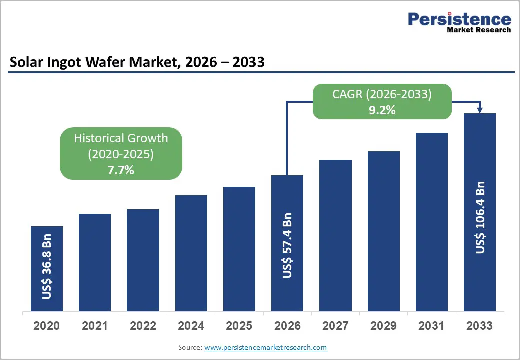
The global solar ingot wafer market size is valued at US$ 57.4 Bn in 2026 and is projected to reach US$ 106.4 Bn by 2033, growing at a CAGR of 9.2% between 2026 and 2033.
This robust growth trajectory is primarily powered by record-breaking global photovoltaic (PV) installations, sweeping government-backed renewable energy mandates, and the industry's decisive migration toward high-efficiency n-type silicon cell architectures. According to the International Energy Agency (IEA), global PV capacity additions reached an unprecedented 601 GW in 2024, up from 465 GW in 2023, with cumulative installed global PV capacity crossing 2.2 terawatts (TW) at the start of 2025.
Key Industry Highlights:
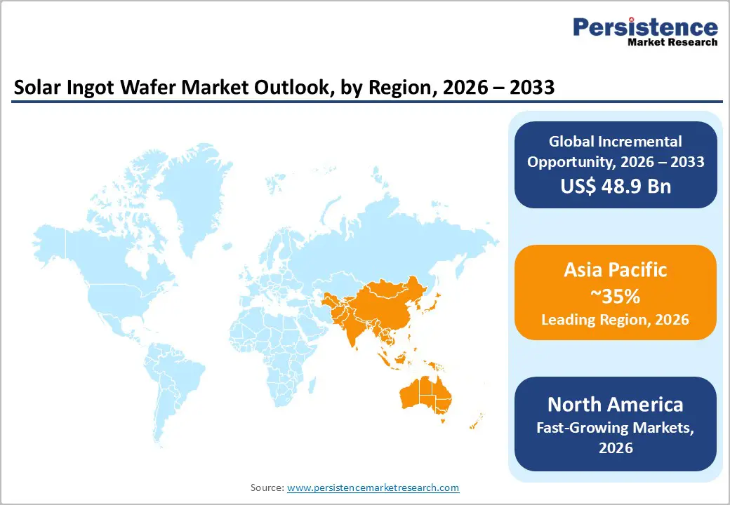
- Leading Region: Asia Pacific leads the global Solar Ingot Wafer market, with China controlling over 80% of global manufacturing capacity. Vertically integrated supply chains, cost leadership, and massive scale investments across ingot and wafer production anchor the region's dominance through 2033.
- Fastest Growing Region: The United States is the primary driver of solar ingot wafer demand in North America, supported by transformational federal policy frameworks. Despite this policy momentum, SEIA confirmed that no commercial-scale ingot or wafer facility was operational in the U.S. as of late 2024, with 3.3 GW under construction against at least 21 GW of announced wafer capacity plans.
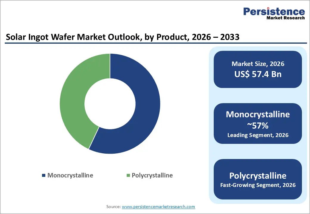
- Dominant Segment: Monocrystalline wafers dominate the Product Type category with approximately 57% revenue share as of 2025, driven by the exclusive compatibility of monocrystalline substrates with next-generation TOPCon, HJT, and IBC n-type solar cell architectures delivering up to 26.7% efficiency.
- Fastest Growing Segment: Diamond Wire Sawing is the fastest-growing Cutting Method segment, commanding an estimated ~80% global adoption rate, driven by lower silicon kerf loss, superior surface quality, higher throughput, and cost efficiency advantages over traditional Loose Abrasive Slurry Sawing.
- Key Market Opportunity: The confirmation of a 25% investment tax credit for U.S. solar ingot and wafer manufacturing under the CHIPS Act (2022) and complementary IRA Section 45X credits have unlocked at least 21 GW of planned domestic U.S. wafer capacity, representing a landmark near-term market entry opportunity.
| Key Insights | Details |
|---|---|
| Solar Ingot Wafer Market Size (2026E) | US$ 57.4 Bn |
| Market Value Forecast (2033F) | US$ 106.4 Bn |
| Projected Growth (CAGR 2026 to 2033) | 9.2% |
| Historical Market Growth (CAGR 2020 to 2025) | 7.7% |
Market Dynamics
Drivers - Record Global Solar PV Deployment Sustaining Wafer Demand
The unprecedented pace of global solar photovoltaic installations is the foremost structural driver of demand for solar ingots and wafers. According to the International Energy Agency (IEA), annual global PV capacity additions reached a record 601 GW in 2024, surpassing the 465 GW installed in 2023, and bringing cumulative global PV installed capacity above 2.2 TW at the start of 2025. With national energy transition targets across Asia Pacific, Europe, and North America mandating aggressive renewable deployment through the 2030s, the demand for silicon wafers the foundational input of every solar cell is set for sustained multi-year growth. Utility-scale solar farm proliferation, rising rooftop solar adoption, and distributed energy projects all channel demand upstream to the ingot and wafer segment.
Shift to High-Efficiency N-Type Cell Architectures Elevating Wafer Specifications
The rapid industry-wide transition from conventional p-type to high-efficiency n-type solar cell technologies specifically TOPCon (Tunnel Oxide Passivated Contact), HJT (Heterojunction Technology), and IBC (Interdigitated Back Contact) is fundamentally reshaping the wafer procurement landscape. According to Fraunhofer ISE, the record conversion efficiency for monocrystalline silicon solar cells stands at 26.7%, establishing the technical superiority of monocrystalline-based n-type architectures. JA SOLAR Technology Co., Ltd. disclosed that by end-2024, its actual n-type battery production capacity reached 70 GW, representing a dominant share of its overall manufacturing mix. N-type cells require ultra-high-purity monocrystalline wafers with exceptional minority carrier lifetimes and surface passivation compatibility, commanding premium pricing and driving continued R&D investment in advanced Czochralski crystal growth and large-format ingot slicing technologies.
Restraints - Extreme Geographic Concentration of Manufacturing in China
The global solar ingot and wafer supply chain faces a profound structural risk stemming from the overwhelming concentration of production capacity in China. According to Wood Mackenzie, China controls over 80% of global solar manufacturing capacity across all supply chain tiers, including ingots, wafers, cells, and modules. This dependency exposes downstream manufacturers to supply disruptions from geopolitical tensions, trade policy shifts, and export restrictions. The U.S. Solar Energy Industries Association (SEIA) confirmed that the United States had no commercial-scale ingot and wafer manufacturing operational as of late 2024, with merely 3.3 GW of capacity under construction. This single-country concentration stifles regional supply chain resilience amplifies import dependency, and limits pricing competition across global markets.
High Capital Intensity and Silicon Kerf Loss in Wafer Production
The manufacturing of high-purity silicon ingots and their precision slicing into wafers demand enormous capital investment in Czochralski furnaces, crystal pulling equipment, and advanced wire-sawing systems. Silicon kerf loss the raw material wasted during the cutting process remains a persistent efficiency challenge in traditional production setups. Published research in peer-reviewed journals has estimated that kerf losses in conventional wire-saw processes can account for up to 40-45% of total silicon input, materially inflating raw material and production costs. Polysilicon feedstock price volatility adds further cost uncertainty, while the capital expenditure required to commission a new integrated ingot-wafer facility can run to several hundred million dollars, creating high barriers to entry and limiting competitive diversification in the global market.
Opportunities - U.S. Domestic Supply Chain Build-Out Under CHIPS Act and Inflation Reduction Act
The finalization of solar ingot and wafer investment incentives under U.S. federal policy creates a transformational near-term opportunity for market participants. In October 2024, the U.S. Department of Treasury and the Internal Revenue Service (IRS) confirmed that solar ingot and wafer manufacturing facilities and equipment qualify for a 25% Advanced Manufacturing Investment Tax Credit (ITC) under the final rules of the CHIPS and Science Act of 2022, effective retroactively from December 23, 2024. Additionally, the Inflation Reduction Act (IRA) of 2022 provides Section 45X production tax credits for domestically manufactured solar components. SEIA reported that since IRA's passage, industry participants have collectively announced intent to produce at least 21 GW of wafers and 10 GW of ingots in the U.S.
India's PLI-Driven Upstream Solar Manufacturing Expansion
India represents one of the most significant emerging opportunities for solar ingot and wafer manufacturers, underpinned by a comprehensive and well-funded government incentive architecture. Under India's Production Linked Incentive (PLI) Scheme for Solar PV Manufacturing, ingot-wafer production capacity reached 2.2 GW operational as of June 2025, with total PLI awards across Tranche I and II reaching 48 GW of integrated manufacturing. India's Ministry of New and Renewable Energy (MNRE) has set a target of achieving 500 GW of total renewable energy capacity by 2030, which structurally demands scaling of the domestic upstream solar supply chain. India's high import dependence on wafers and cells creates urgency for domestic capacity, and the PLI scheme's graded financial incentives for integrated polysilicon-to-module manufacturing directly encourage upstream investment.
Category-wise Analysis
Product Type Insights
The monocrystalline segment leads the global Solar Ingot Wafer market, commanding approximately 57% of total market revenue share as of 2025. This dominance is anchored in monocrystalline wafers' measurably superior characteristics: Fraunhofer ISE has established a benchmark conversion efficiency of 26.7% for monocrystalline silicon solar cells significantly above polycrystalline counterparts alongside better performance in low-light and high-temperature conditions, longer operational lifetimes, and a smaller physical footprint per watt. The wholesale industry transition to n-type TOPCon, HJT, and IBC cell architectures, each exclusively requiring monocrystalline substrates for optimal performance, has further entrenched segment leadership. Large-format monocrystalline wafers such as the M10 (182 mm) and G12 (210 mm) formats are becoming the manufacturing standard.
Application Insights
The Mono Solar Cells application segment dominates the Solar Ingot Wafer market, directly correlating with the upstream predominance of monocrystalline wafers in the production mix. As the industry transitions toward high-efficiency n-type cell technologies, mono-based cells account for the majority of new solar cell manufacturing capacity globally. JA SOLAR Technology Co., Ltd. reported that by end-2025, its n-type cell capacity which exclusively utilizes monocrystalline wafers reached 70 GW, highlighting the structural alignment between upstream monocrystalline wafer demand and downstream Mono Solar Cell fabrication. Mono Solar Cells based on TOPCon architectures are achieving mass-production efficiencies exceeding 24-25%, significantly outperforming Multi Solar Cell alternatives in both residential and utility-scale deployments.
Cutting Method Insights
The Diamond Wire Sawing (DWS) segment has become the overwhelmingly dominant cutting method in solar wafer manufacturing globally, with an estimated market adoption rate of approximately 80% of total wafer cutting operations, displacing the traditional Loose Abrasive Slurry Sawing (LASS) method. Diamond wire sawing offers decisive technical and economic advantages: higher cutting throughput, significantly reduced kerf loss, superior wafer surface quality, lower silicon waste per wafer, and substantially lower per-unit production costs at scale. A 2025 peer-reviewed study published in Applied Energy confirmed that ongoing improvements in DWS including finer wire diameters and higher cutting speeds are enabling continued kerf-loss reduction critical to cost competitiveness in solar manufacturing.
Regional Insights
North America Solar Ingot Wafer Market Trends
The United States is the primary driver of solar ingot wafer demand in North America, supported by transformational federal policy frameworks. The U.S. Department of Treasury confirmed in October 2024 that solar ingot and wafer production qualifies for a 25% Advanced Manufacturing Investment Tax Credit under the CHIPS and Science Act of 2022, effective from December 2024.
Despite this policy momentum, SEIA confirmed that no commercial-scale ingot or wafer facility was operational in the U.S. as of late 2024, with 3.3 GW under construction against at least 21 GW of announced wafer capacity plans. This gap represents a near-term structural investment opportunity. The U.S. innovation ecosystem spanning advanced crystal growth research at national laboratories and university partnerships positions North America for technology-led differentiation in premium-grade solar wafer manufacturing through the late 2020s.
Europe Solar Ingot Wafer Trends
Europe's solar ingot wafer market is underpinned by the European Union's binding renewable energy regulatory framework. The revised EU Renewable Energy Directive (RED III) mandates that at least 42.5% of EU energy consumption must come from renewable sources by 2030, creating durable long-term demand for photovoltaic components including silicon wafers.
However, European solar manufacturing expansion has faced significant headwinds in cost competitiveness against Asian producers. According to online sources, several ambitious 2024 European manufacturing capacity plans proved difficult to execute against Chinese price competition. Siltronic AG (Germany), which completed construction of its new advanced Singapore fabrication facility for high-purity silicon wafers, illustrates the hybrid localization strategy adopted by European players.
Asia Pacific Solar Ingot Wafer Trends
Asia Pacific is unequivocally the dominant and fastest-growing region in the global solar ingot wafer market. China controls over 80% of global solar manufacturing capacity across the entire supply chain, as documented by Wood Mackenzie, giving Chinese producers unparalleled advantages in cost, scale, and vertical integration from polysilicon through finished modules. In the first half of 2025, cells and wafers accounted for 42% of China's total solar exports, according to PV Tech, demonstrating the upstream manufacturing base's export significance.
India is the region's fastest-growing upstream market, with 2.2 GW of ingot-wafer capacity operational by June 2025 under the PLI Scheme, according to MNRE and industry sources. Japan and South Korea contribute premium-grade silicon wafer capabilities through Sumco Corporation and SK Siltron respectively.
Competitive Landscape
The global Solar Ingot Wafer market exhibits a moderately consolidated structure, with Chinese manufacturers collectively commanding the dominant production share, while semiconductor-grade wafer specialists maintain significant positions in premium segments. Competition is fought across dimensions of manufacturing scale, crystal growth technology, wafer format innovation, purity grade, and unit cost efficiency. Leading strategic trends include aggressive vertical integration from polysilicon to modules pursued by major Chinese producers, R&D investment in large-format M10 and G12 wafer platforms, and geographic diversification into Southeast Asia, India, and the Middle East.
Key Developments:
- In April 2025, JA SOLAR Technology Co., Ltd. announced plans to expand integrated production capacity of ingots, wafers, solar cells, and modules with an investment of 10.391 billion Yuan, reinforcing its vertical integration roadmap and n-type product line expansion strategy.
- In October 2024, The U.S. Department of Treasury and the Internal Revenue Service (IRS) finalized rules confirming that solar ingot and wafer manufacturing facilities qualify for a 25% investment tax credit under the CHIPS Act, catalyzing renewed domestic manufacturing investments with 21 GW of wafer capacity already announced.
Companies Covered in Solar Ingot Wafer Market
- Shin-Etsu Chemical Co., Ltd
- CETC Solar Energy Holdings Co., Ltd.
- DCH Group
- KONKA SOLAR Cell Co., Ltd
- Sumco Corporation
- Siltronic AG
- GlobalWafers
- JA SOLAR Technology Co., Ltd.
- SK Siltron
- Okmetic
- Others Key Players
Frequently Asked Questions
The global Solar Ingot Wafer market is valued at US$ 57.4 Bn in 2026 and is projected to reach US$ 106.4 Bn by 2033, registering a CAGR of 9.2% over the 2026-2033 forecast period.
The primary demand drivers include record global PV installations reaching 601 GW in 2024 per the IEA and the industry-wide shift to high-efficiency n-type solar cell architectures such as TOPCon and HJT that exclusively require monocrystalline wafers.
The Monocrystalline segment leads with approximately 57% of total market revenue share as of 2025.
Asia Pacific is the dominant region, led by China, which controls over 80% of the global solar supply chain including ingot and wafer production, according to Wood Mackenzie.
Key players include JA SOLAR Technology Co., Ltd., Shin-Etsu Chemical Co., Ltd., GlobalWafers, Sumco Corporation, CETC Solar Energy Holdings Co., Ltd., Siltronic AG, SK Siltron, LONGi Green Energy Technology Co., Ltd., Trina Solar, LDK Solar Technology Co., Ltd., KONKA SOLAR Cell Co., Ltd., Okmetic, DCH Group, and SN Materials, among others.


