


- Hardware & Software IT Services
- PCB Design Software Market
PCB Design Software Market Size, Share, and Growth Forecast 2026 - 2033
PCB Design Software Market by Deployment (Cloud, On-premise), Component (Software, Service), Application (Computer & Consumer Electronics, Telecommunication Equipment, Medical Devices, Industrial Equipment, Automotive Components, Aerospace & Defense, Safety and Security Equipment, Others), and Regional Analysis, 2026 - 2033
PCB Design Software Market Size and Trend Analysis
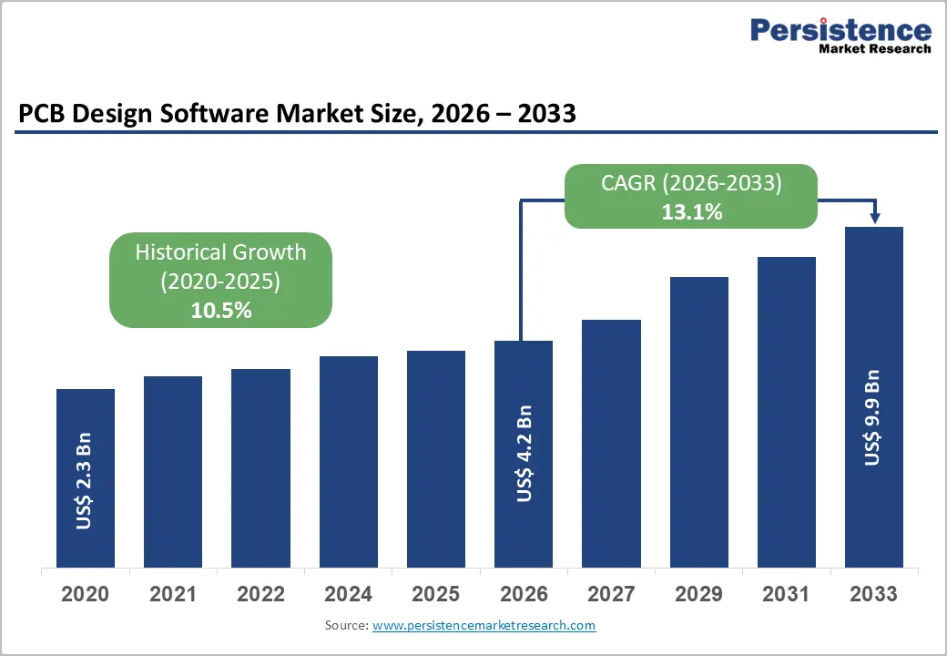
The global PCB design software market size is expected to be valued at US$ 4.2 billion in 2026 and projected to reach US$ 9.9 billion by 2033, growing at a CAGR of 13.1% between 2026 and 2033. Strong growth in complex electronics, driven by 5G, Internet of Things (IoT), electric vehicles (EVs), and advanced industrial automation, is pushing design teams toward more capable electronic design automation platforms that can handle high-speed, high-density printed circuit boards.
At the same time, leading vendors such as Altium, Siemens EDA, Cadence Design Systems, Inc., and Autodesk Inc. are expanding cloud-enabled collaboration, integrating supply-chain data and manufacturing feedback, and embedding simulation into PCB workflows, which increases the strategic importance and spend on PCB design tools within electronics organizations worldwide. These technology and demand shifts together support sustained double-digit expansion of the PCB design software market over the forecast period.
Key Industry Highlights:
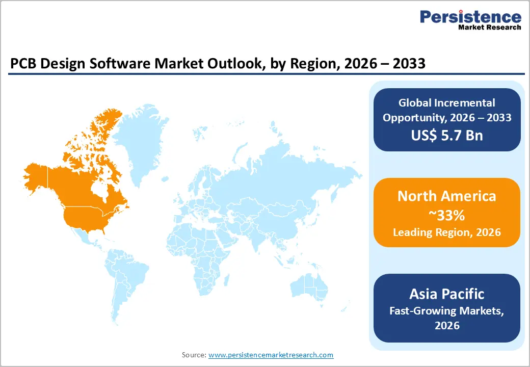
- Leading region: North America leads the PCB design software market due to its concentration of major EDA vendors, high R&D expenditure, and strong demand from semiconductor, aerospace, defense, and cloud infrastructure companies that depend on advanced PCB design capabilities.
- Fastest-growing region: Asia Pacific is the fastest-growing region, driven by its role as the world’s electronics manufacturing hub, rapid expansion of local design teams in China, Japan, South Korea, Taiwan, and India, and rising adoption of professional and cloud-based PCB tools.
- Dominant segment: The software component segment holds the dominant share of the market, exceeding an estimated 65% in 2025, as organizations invest primarily in feature-rich PCB design suites and cloud subscriptions, while services such as training and consulting remain complementary.
- Fastest-growing segment: Cloud deployment is the fastest-growing segment by deployment model, as vendors roll out SaaS and hybrid offerings and customers seek scalable collaboration, lower up-front costs, and easier access to integrated simulation, data management, and supply-chain intelligence.
- Key market opportunity: The largest opportunity lies in cloud-native, AI-enabled PCB design platforms that seamlessly connect design, simulation, supply-chain, and manufacturing, helping organizations shorten development cycles, mitigate component risks, and optimize product cost and quality.
| Key Insights | Details |
|---|---|
| PCB Design Software Market Size (2026E) | US$ 4.2 billion |
| Market Value Forecast (2033F) | US$ 9.9 billion |
| Projected Growth CAGR (2026 - 2033) | 13.1% |
| Historical Market Growth (2020 - 2025) | 10.5% CAGR |
Market Dynamics
Drivers - Proliferation of complex, connected electronic systems across industries
The rapid proliferation of connected devices and high-performance electronics is a primary driver for PCB design software adoption. Industry estimates suggest there were over 31 billion internet-connected devices in 2020, with expectations of reaching around 75 billion by 2025, illustrating the explosion in Internet of Things (IoT) nodes, smart consumer devices, and embedded systems. Automotive electronics content per vehicle is also rising sharply, as advanced driver-assistance systems, infotainment, and electrified powertrains depend on multilayer boards and high-speed interfaces. These trends demand PCB design environments capable of handling dense layouts, signal integrity, power integrity, and electromagnetic compatibility constraints, pushing organizations to upgrade from legacy tools to modern suites from vendors such as Cadence, Synopsys, Siemens EDA, and Altium. As product life cycles shorten and design reuse increases, PCB design software becomes central to sustainable competitive advantage in electronics-intensive sectors.
Shift toward cloud-enabled, collaborative EDA workflows
A second major growth driver is the shift from purely desktop, on-premises PCB design environments to cloud-enabled platforms that support distributed engineering teams and continuous collaboration. Siemens Digital Industries Software has highlighted how integrating AWS cloud capabilities into its PCB toolchain improves global collaboration, security, and time-to-market by enabling geographically dispersed teams to work on the same designs in real time with scalable compute for simulation. Altium LLC reports that more than 5,000 companies and 11,000 users had adopted its Altium 365 cloud platform and Nexar™ ecosystem shortly after launch, underlining strong demand for cloud-based PCB design, data management, and supply-chain integration. Cloud-hosted PCB tools also reduce up-front licensing and hardware costs for small businesses and startups through subscription models, making professional-grade design tools more accessible and accelerating overall market adoption.
Restraints - High cost and complexity of professional PCB design suites
Professional PCB design and broader EDA platforms represent significant investments, particularly for small and medium-sized enterprises. Leading EDA suppliers such as Cadence, Synopsys, Ansys, and Siemens EDA together account for over 90% of global EDA revenues, and their flagship design suites can cost thousands of dollars per seat, with recurring maintenance and upgrade fees. Many tools also require powerful workstations and skilled engineers to fully exploit advanced routing, simulation, and verification capabilities, raising the total cost of ownership. This cost and complexity can delay adoption or expansion of PCB design software licenses among budget-constrained organizations, even when the productivity benefits are clear.
Skilled talent shortage and steep learning curves
Another key restraint is the shortage of experienced PCB designers and the steep learning curve associated with advanced design environments. High-end tools integrate schematic capture, layout, design rule management, 3D visualization, and multiphysics simulation, creating a rich but complex environment that takes time to master. Many electronics manufacturers and design services firms in fast-growing regions such as Asia Pacific report difficulty in hiring engineers with deep expertise in high-speed, high-density PCB design, slowing down the effective deployment of sophisticated software capabilities. This skills gap can limit productivity gains and lead organizations to under-utilize available features, tempering the realized ROI from PCB design software investments.
Opportunity - AI-driven automation and advanced simulation in PCB workflows
One of the most promising opportunities in the PCB design software market lies in integrating artificial intelligence and advanced simulation more deeply into everyday design workflows. Industry analysis of the broader EDA sector notes that core EDA revenues for leading vendors have grown at double-digit CAGRs, supported in part by hardware-based verification and advanced IP, illustrating strong customer willingness to invest in higher-value automation and analysis tools. PCB-focused tools are increasingly adding AI-assisted auto-routing, design-for-manufacturing checks, and real-time signal and power integrity analysis, as highlighted by vendor communications and product roadmaps. As complexity rises in 5G infrastructure, data centers, and EV power electronics, design teams will seek out platforms that can automatically propose optimal topologies, detect layout issues early, and simulate behavior across electrical, thermal, and mechanical domains, creating sizable upsell and cross-sell opportunities for software providers.
Cloud-native platforms connecting design, supply chain, and manufacturing
A second major opportunity is the evolution of cloud-native PCB design platforms that tightly connect design data with supply-chain and manufacturing ecosystems. Altium’s Nexar cloud platform and Octopart® component search engine exemplify this trend, offering access to millions of electronic component CAD models and real-time supply data that can be incorporated directly into PCB designs. KLA Corporation has launched cloud-based Frontline Cloud Services to accelerate design-for-manufacturing (DFM) analysis and reduce time-to-market for complex PCBs, illustrating how manufacturers are also moving critical pre-production analysis into the cloud. As design teams look to mitigate component shortages, manage lifecycle risks, and ensure manufacturability across a distributed supplier base, demand will grow for PCB design environments that integrate sourcing, compliance, and fabrication feedback, opening new revenue streams around data services, analytics, and collaborative workflows.
Category-wise Analysis
Deployment Insights
On-premise deployment currently accounts for the largest share of the PCB design software market, with an estimated share above 60% in 2025, reflecting longstanding enterprise investments in desktop and network-licensed tools integrated into local IT environments. Large semiconductor, aerospace, and defense organizations often maintain strict control over design data for security and compliance reasons, reinforcing the dominance of on-premise deployments.
At the same time, vendors such as Siemens, Altium, and Autodesk are increasingly offering hybrid models where core layout tools remain desktop-based but collaborate through cloud services for data management, version control, and remote access. This ensures that on-premise solutions remain central to mission-critical workflows while gradually blending into cloud-connected ecosystems.
Component Insights
The software component segment represents the clear leader in the PCB design software market, accounting for an estimated 65% or more of total revenues in 2025, driven by license and subscription sales of layout, schematic, and analysis tools. Industry commentary on the wider EDA space shows that core design software, including PCB layout, schematic capture, and related IP, constitutes the majority of vendor revenues, with services playing a complementary but smaller role.
As PCB complexity increases, customers prioritize feature-rich, regularly updated software platforms from vendors such as Cadence Design Systems, Inc., ANSYS, Inc., Siemens, Altium Limited, and Autodesk Inc., reinforcing the revenue dominance of software licenses and cloud subscriptions over consulting, training, and integration services.
Application Insights
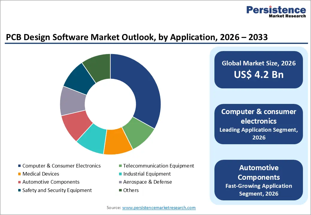
Computer & consumer electronics is the leading application segment for PCB design software, capturing an estimated share of around 34% in 2025, reflecting the enormous volume and diversity of devices such as smartphones, laptops, wearables, gaming systems, and smart home products. Analysts estimate that billions of smart, connected consumer devices are in use globally, and platforms like Altium 365 and Nexar were explicitly launched to serve this rapidly expanding electronics design community.
At the same time, applications in telecommunication equipment, automotive components, and industrial equipment are growing quickly due to 5G rollouts, EV electrification, and Industry 4.0 automation, further increasing PCB design complexity and driving upgrades to advanced software solutions across these verticals.
Regional Insights
North America PCB Design Software Market Trends and Insights
North America is a leading regional market for PCB design software, underpinned by the presence of major EDA vendors, high R&D spending, and strong demand from semiconductor, aerospace, defense, and advanced electronics manufacturers. The “big four” EDA suppliers-Cadence, Synopsys, Ansys, and Siemens EDA-are all headquartered or have major operations in the region and collectively account for over 90% of global EDA revenues, reflecting the strategic importance of North America in design tool innovation and commercialization.
The United States also hosts many of the world’s largest technology companies, cloud providers, and semiconductor firms, which invest heavily in PCB and system-level design capabilities to support data centers, networking, high-performance computing, and aerospace programs. Regulatory frameworks around export controls, cybersecurity, and defense procurement further reinforce the use of high-end, secure PCB design environments managed by trusted vendors. North American innovation ecosystems therefore continue to set the pace in advanced PCB design workflows, from AI-assisted routing and verification to cloud-connected collaboration.
Europe PCB Design Software Market Trends and Insights
Europe represents a significant market for PCB design software, driven by strong industrial bases in Germany, France, the United Kingdom, and the Nordic countries, as well as specialization in automotive, industrial automation, medical technology, and aerospace. European semiconductor and electronics firms rely heavily on advanced PCB tools to support safety-critical applications in automotive electronics and industrial controls, where functional safety and electromagnetic compatibility are tightly regulated under EU directives and standards.
The region benefits from a mix of global and local vendors, including Siemens EDA and Zuken with a strong presence in automotive and transportation. Harmonized regulatory frameworks around product safety, environmental compliance, and data protection encourage the adoption of robust design and data-management practices in PCB workflows. As Europe accelerates investments in electric mobility, renewable energy, and digital infrastructure, demand for capable PCB design software that supports high-reliability, high-voltage, and high-speed designs is expected to remain strong.
Asia Pacific PCB Design Software Market Trends and Insights
Asia Pacific is the fastest-growing region for PCB design software, reflecting its dominant position in electronics manufacturing and the rapid expansion of local design capabilities. Countries such as China, Japan, South Korea, Taiwan, and India host extensive electronics and PCB fabrication ecosystems, with many original design manufacturers (ODMs) and original equipment manufacturers (OEMs) engaging in both design and production. As these firms move up the value chain from contract manufacturing to full product development, their reliance on professional PCB design tools from vendors like Altium, Cadence, Siemens, and Zuken is intensifying.
The rollout of 5G networks, growth in smartphone and consumer electronics production, and the rise of local EV, battery, and renewable-energy industries in China and India all contribute to increased PCB design complexity and software demand. Moreover, cloud-based PCB solutions are attractive for emerging engineering teams in ASEAN markets, enabling them to access advanced design and collaboration capabilities without large capital expenditures. As a result, Asia Pacific is expected to post the highest CAGR for PCB design software over 2026 - 2033, while progressively closing the revenue gap with more mature markets.
Competitive Landscape
The PCB design software market is moderately consolidated at the premium tier, where a small group of global EDA vendors capture a substantial share of revenue through comprehensive, end-to-end design platforms. These companies benefit from deep integration across schematic capture, layout, simulation, signal integrity, and system verification, creating high switching costs and long-term enterprise contracts. At the same time, the market remains structurally diverse, with mid-tier and regional providers serving cost-sensitive customers, startups, educational institutions, and specialized workflow requirements.
Competitive strategies increasingly revolve around subscription-based licensing, cloud-native deployment, and scalable collaboration features for distributed engineering teams. Vendors are embedding AI-driven automation to accelerate routing, design rule checks, and optimization, reducing time to market. Deeper integration with component databases, supply chain intelligence, and manufacturing feedback systems is becoming a differentiator, enabling real-time part availability checks and design-for-manufacturability validation. Overall, competition is shifting from standalone tools toward connected, data-driven design ecosystems.
Key Developments:
- January, 2026: Siemens acquired ASTER Technologies to integrate advanced design-for-test capabilities into its PCB design and manufacturing software, enhancing early defect detection, reducing costs, and accelerating time-to-market for electronic systems.
- May, 2025: Siemens released AI-enhanced PADS Pro Essentials and Xpedition Standard PCB design tools to bring cloud-connected, AI-driven electronic design capabilities to small and mid-sized teams, accelerating design cycles and improving collaboration.
- September, 2025: Pentalogix launched ViewMate Essentials, a new CAM package that helps PCB designers view, edit, and prepare manufacturing files, ensuring designs are production-ready and improving collaboration with fabricators and assemblers.
Companies Covered in PCB Design Software Market
- Autodesk Inc.
- ANSYS, Inc.
- Cadence Design Systems, Inc.
- Siemens EDA
- Zuken
- Altium Limited
- NATIONAL INSTRUMENTS CORP.
- Labcenter Electronics
- Novarm Limited
- KLA Corporation
- Synopsys Inc.
- EasyEDA
- Pentalogix
- KiCad (community driven open source PCB design suite)
- SolidWorks PCB (from Dassault Systèmes)
Frequently Asked Questions
The global PCB design software market is projected to reach approximately US$ 4.2 billion in 2026.
Demand is driven by increasing complexity of electronic systems, growth of IoT and 5G devices, rising automotive electronics integration, and adoption of cloud-based collaborative design tools.
North America leads the market due to strong presence of EDA vendors and high R&D spending across semiconductor, aerospace, and cloud infrastructure sectors.
The key opportunity lies in AI-enabled, cloud-native PCB design platforms integrating simulation, supply chain intelligence, and manufacturing feedback.
Major players include Cadence Design Systems, Inc., Synopsys Inc., Siemens EDA, Altium Limited, and Autodesk Inc.


