


- Semiconductor Materials & Components
- Tantalum Sputtering Target Market
Tantalum Sputtering Target Market Size, Share, and Growth Forecast, 2026 - 2033
Tantalum Sputtering Target Market by Purity Type (Low Purity, High Purity), Configuration Type (Planar Targets, Rotatable Targets), Application (Semiconductors, Flat Panel Displays, Solar Cells, Others), and Regional Analysis 2026 - 2033
Tantalum Sputtering Target Market Size and Trends Analysis
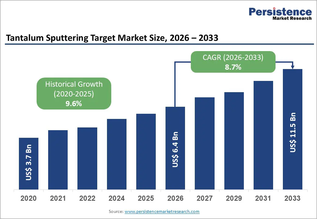
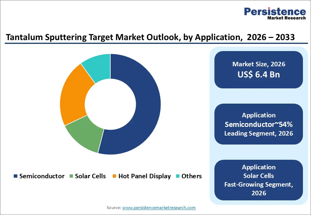
The global tantalum sputtering target market size is likely to be valued at US$6.4 billion in 2026 and is expected to reach US$11.5 billion by 2033, growing at a CAGR of 8.7% during the forecast period from 2026 to 2033, driven by the escalating complexity of semiconductor architectures, particularly in logic and memory chips, where high-purity tantalum is critical for diffusion barriers. The proliferation of next-generation flat-panel displays and thin-film solar technologies is also driving sustained demand for large-area coating solutions.
Key Industry Highlights:
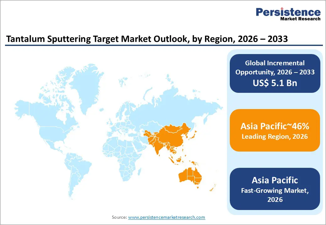
- Leading Region: Asia Pacific is projected to lead due to its dense concentration of semiconductor fabrication facilities, advanced packaging ecosystems, and vertically integrated electronics manufacturing clusters, accounting for approximately 46% share.
- Fastest-growing Region: Asia Pacific is anticipated to grow fastest due to aggressive fab capacity expansion, national semiconductor self-sufficiency programs, and scaling logic and memory production.
- Leading Application: Semiconductors are expected to lead, accounting for approximately 54%, driven by tantalum’s critical function as a diffusion barrier and adhesion layer in metallization stacks for logic and memory devices.
- Leading Configuration: Planar targets are projected to dominate with approximately 62%, supported by widespread compatibility with conventional sputtering systems and strong adoption in semiconductor wafer processing.
| Key Insights | Details |
|---|---|
|
Tantalum Sputtering Target Market Size (2026E) |
US$6.4 Bn |
|
Market Value Forecast (2033F) |
US$11.5 Bn |
|
Projected Growth (CAGR 2026 to 2033) |
8.7% |
|
Historical Market Growth (CAGR 2020 to 2025) |
9.6% |
Market Factors - Growth, Barriers, and Opportunity Analysis
Growth Analysis - Advancement in Flat Panel Display Technologies
The transition from conventional LCD architectures toward OLED, QLED, and flexible display platforms is structurally reinforcing demand for high-performance thin-film transistor backplanes. Advanced display stacks require gate electrode materials that combine low electrical resistivity with strong chemical stability to maintain switching precision across densely packed pixel arrays. Tantalum fulfills these requirements, offering superior conductivity and inertness under repeated thermal cycling and plasma exposure. As display resolutions increase and refresh rates accelerate, material uniformity and thin-film consistency become critical yield determinants. This underscores the importance of high-purity tantalum sputtering targets that enable defect-minimized deposition across large substrates used in next-generation consumer electronics and automotive display modules.
The shift toward larger television panels and integrated automotive cockpit displays expands substrate dimensions, increasing coating surface area per production cycle. This dynamic drives the adoption of rotatable sputtering targets, which improve material utilization efficiency and reduce downtime during target changes. Higher utilization rates directly influence cost-per-square-meter deposition economics, particularly in capital-intensive display fabrication environments where throughput optimization governs margin stability. As panel makers pursue thinner form factors and flexible substrates, deposition systems must deliver uniform coverage over increasingly complex geometries, reinforcing demand for engineered tantalum targets optimized for large-area, high-precision coating processes.
Escalating Semiconductor Architecture Complexity and Advanced Node Scaling
The progressive scaling of semiconductor architectures toward advanced logic and memory configurations is a primary structural driver for the production of tantalum sputtering targets. As fabrication migrates to increasingly compact geometries, copper interconnect integration requires highly stable diffusion barrier layers to prevent material migration and preserve device integrity. Tantalum and tantalum nitride remain critical in this function due to their chemical stability, adhesion characteristics, and compatibility with plasma-based deposition processes. The transition toward three-dimensional memory stacks and non-planar transistor architectures intensifies deposition precision requirements and multiplies the number of barrier-layer integration steps per wafer. This elevates cumulative target consumption across fabrication lines and reinforces demand for ultra-high-purity tantalum materials capable of meeting defect-control thresholds in advanced manufacturing environments.
The growth of artificial intelligence accelerators, high-performance computing, and advanced connectivity platforms drives both increased wafer starts and greater process complexity. To maintain yield stability amidst shrinking process windows, foundries and integrated device manufacturers focus on ensuring material consistency, controlling grain structure, and minimizing impurities. These demands raise material qualification standards and enhance the strategic role of sputtering target suppliers within the semiconductor capital equipment supply chain.
Barrier Analysis – Recycling Bottlenecks in Secondary Tantalum Recovery
Despite tantalum’s intrinsic material value and recoverability, large-scale recycling from Waste Electrical and Electronic Equipment remains structurally constrained. Extreme component miniaturization, particularly in multilayer capacitors and microelectronic assemblies, complicates mechanical separation and material liberation processes. The encapsulation of tantalum anodes within complex mold resins and composite substrates introduces additional thermal and chemical treatment challenges, increasing process intensity and reducing recovery efficiency. These technical barriers limit the viability of secondary feedstock streams and constrain the development of a circular supply chain capable of offsetting dependence on primary extraction.
From a value-chain standpoint, the lack of sufficient industrial-scale recycling capacity continues to rely on mined concentrates, leaving the market vulnerable to raw material price fluctuations and geopolitical sourcing risks. The growing complexity of processing increases recycling costs, often reducing the profitability compared to sourcing primary materials. Stricter environmental regulations surrounding electronic waste treatment impose greater operational challenges on recyclers, further hindering capacity growth. Together, these factors limit the flexibility of secondary supply and dampen cost-stabilization mechanisms across the overall tantalum sputtering target ecosystem.
Substitution Risk in Safety-Critical Electronic Architectures
Selective material substitution in safety-critical automotive electronics poses a structural restraint on the demand for tantalum-based components. In certain Advanced Driver Assistance Systems, niobium capacitors are increasingly adopted as cost-efficient alternatives where voltage and performance thresholds permit material flexibility. As automotive OEMs prioritize cost optimization across high-volume electronic control units, procurement strategies increasingly evaluate total system cost rather than single-component reliability margins. This recalibration introduces competitive pressure on tantalum in applications where its electrical stability exceeds baseline system requirements, narrowing its addressable niche in specific low-to-mid-voltage modules.
Substitution dynamics impact upstream material demand and introduce volatility into consumption forecasts for specific applications. While tantalum continues to offer superior performance in high-voltage and thermally demanding environments, its selective replacement in cost-sensitive segments leads to reduced volume stability in automotive electronics. This shift aligns with broader platform engineering trends that prioritize modular designs and supplier cost control, which together temper incremental growth potential in certain safety-critical electronic subsystems.
Opportunity Analysis – Closed-Loop Recycling and Urban Mining Integration
The expansion of closed-loop recycling frameworks presents a structurally significant opportunity within the tantalum sputtering target market. As environmental, social, and governance mandates tighten across semiconductor supply chains, fabrication facilities increasingly prioritize targets derived from recycled feedstock. Urban mining initiatives that recover tantalum from spent targets and electronic scrap enable material recirculation while reducing dependence on primary mining inputs. Certified closed-loop systems that encompass collection, refining, and re-fabrication strengthen traceability, enhance compliance with responsible sourcing standards, and align with sustainability objectives embedded within advanced electronics procurement policies.
Vertically integrated recycling capabilities mitigate raw material volatility and improve supply security in a geopolitically sensitive minerals landscape. Recycled tantalum streams are projected to outpace virgin material growth, reflecting structural demand for lower-embedded-carbon and reduced-lifecycle-impact materials. This shift supports margin differentiation for suppliers capable of delivering verified recycled content, while reinforcing long-term resilience and sustainability integration across semiconductor manufacturing ecosystems.
Adoption of Rotatable Targets in Large-Area Coating Applications
The transition toward rotatable sputtering targets in large-area coating environments represents a structurally attractive opportunity for tantalum target manufacturers. Display panels and photovoltaic modules increasingly require uniform thin-film deposition across expansive substrates, driving preference for cylindrical rotatable configurations over conventional planar formats. Rotatable targets deliver material utilization rates approaching 80 percent, substantially exceeding the lower efficiency associated with planar targets. This improvement enhances deposition stability, reduces changeover frequency, and lowers per-unit coating cost, particularly in high-throughput production lines operating continuous or semi-continuous processes.
From a cost-structure perspective, higher utilization directly improves raw material efficiency and reduces waste generation, strengthening overall process economics for display and solar manufacturers. Enhanced target longevity also minimizes downtime and maintenance intervention, supporting productivity gains across large-area vacuum deposition systems. As flat panel and renewable energy value chains prioritize yield optimization, throughput stability, and material conservation, rotatable tantalum targets gain strategic relevance within advanced thin film manufacturing ecosystems. This transition positions cylindrical architectures as a performance-driven upgrade pathway in large-area sputtering infrastructure.
Category–wise Analysis
Configuration Insights
Planar targets are expected to lead, accounting for approximately 62% share in 2026, supported by its entrenched integration across legacy PVD infrastructure in 200mm and a significant portion of 300mm fabrication lines. Established semiconductor and specialty electronics facilities rely on planar cathode architectures due to standardized chamber compatibility, simpler bonding processes, and predictable deposition behavior. Their lower upfront manufacturing complexity and cost profile sustain adoption in R&D environments, pilot production, and lower-volume applications requiring film uniformity and process stability. The installed base advantage, combined with qualification familiarity across mature process nodes, reinforces recurring replacement demand. Despite inherent material utilization constraints, entrenched infrastructure and process continuity preserve this segment’s structural dominance within established semiconductor manufacturing ecosystems.
Rotatable targets are expected to be the fastest-growing segment, driven by cost-of-ownership optimization in high-volume, large-area coating environments. Flat panel display, architectural glass, and solar manufacturers increasingly prioritize cylindrical configurations that deliver up to 80% material utilization and extended campaign lifecycles. Enhanced utilization reduces changeover frequency, lowers downtime in continuous 24/7 operations, and improves overall deposition economics. Reduced arcing and improved thermal management further strengthen process stability in large substrates. As new production capacity emphasizes efficiency and throughput scaling, rotatable targets gain preference in expansion projects where operating cost compression and productivity gains outweigh legacy equipment constraints.
Application Insights
Semiconductors are expected to lead, accounting for approximately 54% of the market in 2026, supported by their indispensable role in copper interconnect barrier stacks for advanced logic and memory devices. Tantalum and tantalum nitride layers remain non-negotiable for preventing diffusion failures across increasingly dense architectures, reinforcing the structural demand driven by AI-driven chip expansion and advanced packaging adoption. As device scaling shifts toward More-than-Moore integration and heterogeneous packaging, sputtering intensity per wafer increases, elevating target consumption across fabrication nodes. Sustained industry growth and qualification rigidity across leading fabs preserve revenue concentration within this application segment.
Solar cells are expected to be the fastest-growing segment in the Tantalum Sputtering Target market, driven by the rapid scale-up of thin-film photovoltaic technologies, including CIGS and emerging perovskite architectures. These platforms require stable, conductive back-contact layers with high corrosion resistance and deposition precision, strengthening the case for tantalum-based coatings. Expanding global solar installation capacity, supported by policy acceleration and declining system costs, is shifting procurement toward durable thin-film materials optimized for large-area substrates. Compared with mature display applications, photovoltaic manufacturing is witnessing faster capacity additions and process localization. This expansion trajectory positions solar as the most dynamic incremental demand vector within the broader application landscape.
Regional Insights
Asia Pacific Tantalum Sputtering Target Market Trends
Asia Pacific is expected to remain the dominant volume leader, accounting for approximately 46% in 2026, and with unparalleled semiconductor and display manufacturing scale. The region is projected to anchor demand through concentrated foundry capacity in advanced logic and memory, alongside extensive flat panel and photovoltaic production ecosystems. Dense clustering of PVD equipment suppliers, target fabricators, and end-use manufacturers is anticipated to strengthen just-in-time delivery models and compress logistics cycles. Structurally competitive cost frameworks and vertically integrated electronics supply chains are likely to preserve production efficiency advantages. Cost-efficient manufacturing structures and vertically integrated electronics supply chains are expected to sustain competitive production economics. Government-backed industrial policies and semiconductor self-sufficiency initiatives are likely to reinforce domestic sourcing and accelerate capacity additions across leading fabrication hubs.
China is projected to shape regional momentum through aggressive semiconductor localization and large-scale solar manufacturing expansion. National subsidy frameworks and capacity buildout programs are expected to elevate domestic consumption of high-purity tantalum targets while fostering rapid technological upgrading among local suppliers. Expanding CIGS and thin-film photovoltaic platforms are anticipated to further diversify application intensity beyond traditional semiconductor demand. Vendor strategies are likely to prioritize purity enhancement, bonding precision, and scale-driven cost optimization to compete within an increasingly consolidated yet technologically advancing regional landscape. In response, suppliers are likely to emphasize incremental gains in material purity, bonding accuracy, and scale-based cost optimization to remain competitive within an increasingly consolidated and technologically advancing regional environment.
North America Tantalum Sputtering Target Market Trends
North America is set to maintain its role as a strategic center of innovation and technological leadership, supported by its dense network of advanced semiconductor design and fabrication ecosystems. The region is positioned to capture an outsized share of premium, ultra-high-purity tantalum targets as cutting-edge logic and memory processes continue to scale. Accelerated fabrication build-outs under policy initiatives such as the CHIPS and Science Act are expected to structurally increase domestic consumption of high-specification tantalum consumables. At the same time, rigorous conflict mineral disclosure rules and export control regimes are likely to strengthen traceability and compliance standards, advantaging suppliers with vertically integrated refining, bonding, and precision machining capabilities. Ongoing supply chain realignment is anticipated to reduce reliance on trans-Pacific sourcing and reinforce localized procurement models.
The U.S. is projected to anchor regional momentum by directing capital flows, shaping compliance frameworks, and guiding deployment of advanced semiconductor nodes. Major fabrication investments across states such as Arizona, Texas, and Ohio are expected to heighten demand for barrier-layer materials qualified for sub-advanced processes, reinforcing the premium positioning of domestic suppliers. Regulatory oversight of critical mineral sourcing and export-sensitive semiconductor technologies is likely to accelerate consolidation around transparent, standards-aligned value chains. In response, vendors are prioritizing localized bonding operations, precision machining, and integrated recycling capabilities to support onshore fabrication clusters with minimized logistics friction. The convergence of policy stimulus, innovation concentration, and manufacturing reshoring is therefore expected to sustain North America’s leadership in high-performance tantalum target applications.
Europe Tantalum Sputtering Target Market Trends
Europe is poised to remain a technically sophisticated, engineering-centric market, accounting for roughly one-fifth of global demand for Tantalum Sputtering Targets. This position is underpinned by strong activity in automotive electronics, industrial optics, and advanced materials processing. Regional consumption is expected to closely track developments in electric vehicle power electronics, smart manufacturing automation, and high-precision thin-film applications, where thermal resilience and long-term reliability are essential. Policy instruments such as the European Chips Act, along with coordinated semiconductor expansion programs, are set to strengthen domestic fabrication and advanced packaging capabilities. Concurrently, circular-economy regulations and Critical Raw Materials policy frameworks are likely to accelerate the integration of recycled tantalum into standard procurement channels, redefining sourcing criteria and heightening traceability expectations across the value chain.
Germany is expected to lead regional momentum, driven by its strength in automotive electronics, aerospace systems, and high-value thin-film engineering. The expansion of industrial electrification and electric drivetrain production is expected to increase demand for durable barrier layers and coating materials suitable for high-reliability power modules. Regulatory convergence under REACH and broader sustainability directives is likely to raise benchmarks for material purity and lifecycle transparency, advantaging suppliers with integrated refining and recycling capabilities. Market participants are therefore expected to prioritize closed-loop material recovery models and advanced coating technologies to support growth in OLED applications and precision optics manufacturing clusters. This alignment of regulatory rigor, vehicle electrification, and deep materials engineering expertise should preserve Europe’s distinct structural position within the global market.
Competitive Landscape
The global tantalum sputtering target market is moderately consolidated, with leadership concentrated among global suppliers such as JX Nippon Mining & Metals, Tosoh Corporation, Plansee, Honeywell, and CXMET. These incumbents exert functional influence across the value chain through control over high-purity refining, metallurgical processing, and semiconductor-grade qualification, shaping procurement standards and technical benchmarks for advanced logic, memory, and display applications. High entry barriers linked to conflict-free raw material access, process know-how, and stringent customer validation cycles reinforce their structural positioning and limit competitive displacement.
Competitive differentiation is defined by vertical integration and solution depth: leading suppliers emphasize end-to-end offerings that integrate refining, target fabrication, bonding services, chamber component support, and spent target reclamation, while smaller regional participants focus on cost-competitive supply or niche applications such as architectural glass coating and lower-tier electronics. Industry dynamics reflect selective consolidation, ecosystem alignment with major fabrication clusters, and a gradual shift toward service-led and recycling-integrated business models, reinforcing scale advantages and tightening alignment between materials engineering capability and long-term supply agreements.
Key Industry Highlights:
- In February 2026, Nanografi Advanced Materials introduced high-purity (99.99%) Tantalum Oxide Sputtering Targets for R&D. This enhances scalability from small-scale research to large substrate production with precise growth control.
- In January 2026, TANIOBIS GmbH completed manufacturing expansion at the Map Ta Phut plant in Thailand. Boosts local production capacity for functional tantalum to meet surging demand in the Asia-Pacific hub.
- In December 2025, TECHCET reported a +8% year-over-year revenue growth in sputtering targets reaching $1.45B. Driven by steep increases in source metal costs and the critical role of PVD in advanced semiconductor manufacturing.
Companies Covered in Tantalum Sputtering Target Market
- JX Advanced Metals
- Materion Corporation
- Tosoh SMD, Inc.
- Honeywell Electronic Materials
- Linde plc
- H.C. Starck Solutions
- Plansee SE
- ULVAC, Inc.
- Global Advanced Metals
- Mitsui Mining & Smelting
- Sumitomo Chemical
- KFMI (Konfoong Materials International)
- Grikin Advanced Materials
- CXMET
- Stanford Advanced Materials
- Angstrom Sciences
Frequently Asked Questions
The global tantalum sputtering target market is projected to be valued at US$6.4 billion in 2026 and is expected to reach US$11.5 billion by 2033, driven by escalating semiconductor architecture complexity and the proliferation of next-generation flat panel displays and thin-film solar technologies.
As logic and memory devices scale to advanced nodes, the need for ultra-thin, highly stable copper diffusion barriers intensifies. Tantalum and tantalum nitride are critical for this function due to their chemical stability and adhesion properties, and the transition to 3D architectures multiplies barrier layer integration steps, directly increasing target consumption per wafer.
The tantalum sputtering target market is forecast to grow at a CAGR of 8.7% from 2026 to 2033, reflecting sustained demand from semiconductor fabs, display panel makers, and the ramp-up of thin-film photovoltaic manufacturing.
Asia Pacific is both the leading and fastest-growing regional market, accounting for approximately 46% share, underpinned by its dense concentration of semiconductor fabs, advanced display manufacturing, and aggressive fab capacity expansion driven by national self-sufficiency programs in China, Taiwan, and South Korea.
The tantalum sputtering target market is moderately consolidated, with leadership concentrated among vertically integrated suppliers such as JX Advanced Metals, Tosoh SMD, Materion Corporation, and Plansee SE. These players control high-purity refining and semiconductor-grade qualification. Honeywell Electronic Materials and H.C. Starck Solutions are also significant, competing through material science expertise and closed-loop recycling services.


