


- Specialty & Fine Chemicals
- Etching Chemicals Market
Etching Chemicals Market Size, Share, and Growth Forecast, 2026 – 2033
Etching Chemicals Market by Material Type (Hydrofluoric Acid, Nitric Acid, Sulfuric Acid, Phosphoric Acid, Ferric Chloride), Etching Type (Wet Etching, Dry Etching, Anisotropic Etching, Isotropic Etching), and Regional Analysis for 2026 – 2033
Etching Chemicals Market Size and Trends Analysis
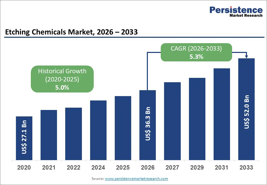
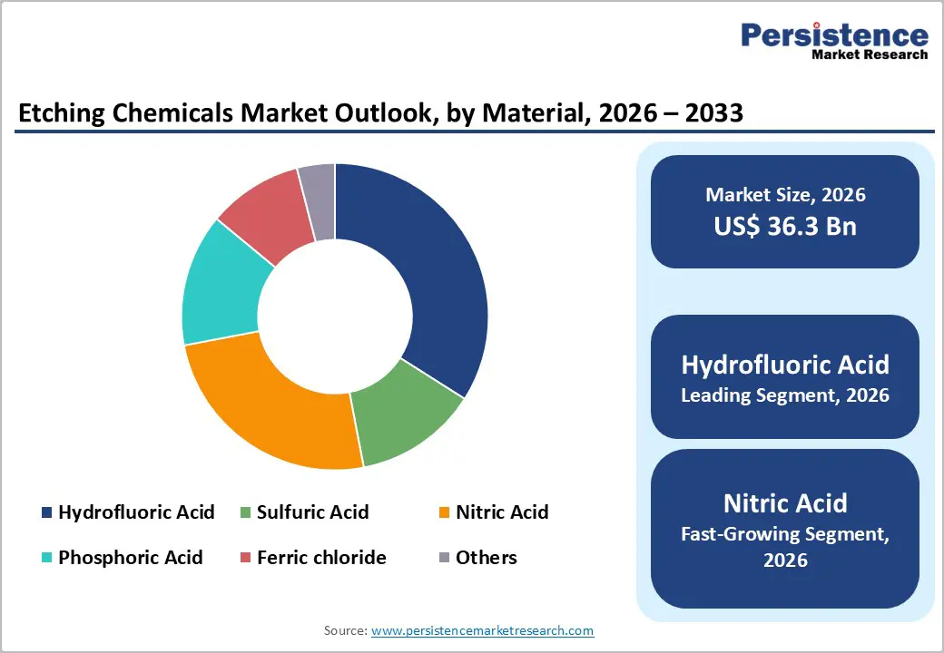
The global etching chemicals market size is likely to be valued at US$36.3 billion in 2026 and is expected to reach US$52.0 billion by 2033, growing at a CAGR of 5.3% during the forecast period from 2026 to 2033, driven by increasing demand from semiconductor manufacturing, PCB fabrication, and electronics sectors, fueled by the adoption of advanced semiconductor nodes, high-density packaging, and precision fabrication technologies. Expanding investments in 5G, AI, IoT, and high-performance computing are accelerating the need for advanced etching chemicals.
The rapid integration of electronics in electric vehicles and automotive sensors is increasing demand for these components. Technological advancements, including dry etching, anisotropic etching, and specialty etchants, are enhancing process precision, yield, and efficiency, while regulatory pressures and the shift toward eco-friendly and low-toxicity chemicals are encouraging innovation and sustainable solutions.
Key Industry Highlights:
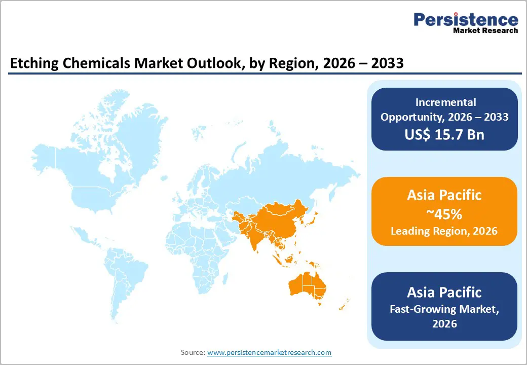
- Leading Region: Asia Pacific is anticipated to be the leading region, accounting for a market share of 45% in 2026, driven by strong semiconductor manufacturing capacity, cost-efficient production ecosystems, supportive government policies, and rapid adoption of advanced electronics and sustainable processing technologies.
- Fastest-growing Region: Asia Pacific is likely to be the fastest-growing region in the etching chemicals industry in 2026, supported by the rapid expansion of semiconductor and electronics manufacturing, strong government-led industrial policies, and increasing investments in advanced fabrication facilities.
- Leading Material Type: Hydrofluoric acid is projected to represent the leading material type in 2026, accounting for 35% of the revenue share, driven by its essential role in silicon wafer and oxide etching in semiconductor manufacturing.
- Leading Etching Type: Wet etching is expected to be the leading etching type, accounting for over 40% of the revenue share in 2026, owing to its cost efficiency, process simplicity, and widespread adoption in large-scale semiconductor and PCB fabrication.
| Report Attribute | Details |
|---|---|
|
Etching Chemicals Market Size (2026E) |
US$36.3 Bn |
|
Market Value Forecast (2033F) |
US$52.0 Bn |
|
Projected Growth (CAGR 2026 to 2033) |
5.3% |
|
Historical Market Growth (CAGR 2020 to 2025) |
5.0% |
Market Factors – Growth, Barriers, and Opportunity Analysis
Growth Analysis - Technological Advancements in Semiconductor Manufacturing
Chipmakers move toward smaller nodes and higher circuit density. Advanced semiconductor devices require precise material removal with minimal defects, making high-purity etching chemicals essential. Processes such as wafer thinning, oxide removal, and pattern transfer rely heavily on acids, including hydrofluoric and nitric acids. As logic and memory chips evolve, etching accuracy directly affects yield, performance, and reliability, thereby increasing the consumption of specialized wet and dry etching chemistries across fabrication stages.
The shift toward advanced architectures such as FinFETs, 3D NAND, and gate-all-around transistors has increased process complexity. These designs demand highly selective and controllable etching solutions to handle multilayer structures and delicate materials. Semiconductor manufacturers are investing heavily in process optimization, increasing demand for innovative etching chemicals with improved selectivity and consistency. As fab capacity expands, especially in Asia Pacific, the need for advanced etching solutions continues to accelerate market growth.
Regulatory Changes Promoting Eco-Friendly Practices
Governments across major manufacturing regions are enforcing stricter regulations on chemical emissions, wastewater discharge, and hazardous material handling. These policies are pushing semiconductor and electronics manufacturers to adopt cleaner etching processes and environmentally compliant chemicals. Chemical suppliers are investing in the development of low-toxicity, recyclable, and low-discharge etching solutions that meet regulatory standards while maintaining process efficiency.
Sustainability initiatives by electronics brands are accelerating the transition to greener manufacturing practices. Companies are increasingly prioritizing suppliers that offer eco-friendly etching chemistries and closed-loop recycling systems. This regulatory and corporate focus on sustainability is reshaping product portfolios across the etching chemicals market. Manufacturers that align with evolving environmental norms gain competitive advantages, while regulatory compliance catalyzes innovation and long-term market expansion.
Barrier Analysis - Environmental and Health Hazards from Chemical Usage
Chemicals such as hydrofluoric acid and nitric acid are highly corrosive and toxic and require strict handling, storage, and disposal procedures. Exposure risks to workers and potential environmental contamination increase operational complexity and compliance costs for manufacturers. These safety concerns often lead to stringent workplace regulations, higher insurance expenses, and increased investments in protective infrastructure. Manufacturers must implement specialized training programs and continuous safety audits, increasing operational overhead. Regulatory inspections and mandatory reporting extend production timelines and raise administrative burdens, particularly in semiconductor-grade chemical manufacturing.
Improper disposal of etching waste can result in soil and water pollution, attracting regulatory penalties and reputational damage. Small and mid-scale manufacturers, particularly in emerging markets, may struggle to meet safety and environmental compliance standards. This limits adoption and slows market penetration in certain regions. The need for advanced waste treatment, chemical neutralization, and real-time effluent monitoring systems significantly increases capital expenditures. These requirements raise entry barriers for new players and constrain capacity expansion.
Raw Material Price Volatility and Supply Chain Constraints
Core inputs such as fluorine-based compounds, acids, and specialty chemicals are subject to fluctuating prices due to supply-demand imbalances, geopolitical tensions, and energy cost variations. These fluctuations directly affect production costs and profit margins for chemical manufacturers, thereby complicating long-term pricing strategies. In semiconductor-grade chemicals, even minor cost changes significantly impact overall manufacturing economics due to stringent purity requirements. Compliance costs associated with sourcing certified raw materials amplify cost pressures, limiting pricing flexibility in highly competitive electronics and semiconductor markets.
Supply chain disruptions exacerbate this issue, particularly for high-purity chemicals required in semiconductor fabrication. Dependence on limited suppliers and regional concentration of raw material sources increases vulnerability to trade restrictions and logistical delays. Such uncertainties can lead to inconsistent supply for end users, thereby affecting fab operations and production schedules. Extended lead times and inventory buffering requirements increase working capital burdens for manufacturers. Price volatility and supply risks constrain market scalability and investment confidence.
Opportunity Analysis - Shift to Eco-Friendly and Low-Discharge Etching Solutions
Semiconductor and electronics manufacturers are increasingly focused on reducing chemical waste, water consumption, and hazardous emissions. This has accelerated demand for environmentally sustainable etching chemistries, including recyclable acids, biodegradable formulations, and low-effluent solutions that comply with stringent environmental standards. Growing adoption of closed-loop chemical management systems supports this shift by enabling the reuse and recovery of etchants. Regulatory mandates on wastewater discharge and chemical handling are pushing fabs to replace conventional formulations. Multinational electronics brands are embedding sustainability requirements into supplier contracts, increasing market demand.
Chemical manufacturers that invest in green innovations gain competitive advantages by meeting regulatory requirements and customer sustainability goals. Eco-friendly etching solutions also help reduce long-term compliance and waste treatment costs for end users. Improved process efficiency and reduced chemical loss enhance operational productivity in semiconductor fabs. Manufacturers offering sustainable portfolios can secure long-term supply agreements with leading electronics and automotive companies. Green solutions support corporate ESG targets, improving brand positioning and investor confidence.
Technological Convergence in Advanced Packaging
Next-generation packaging solutions demand greater precision and material compatibility. Technologies such as 3D integration, chiplets, fan-out wafer-level packaging, and heterogeneous integration require highly controlled etching to enable fine interconnects and high-density layouts. These processes involve complex substrates, including silicon, glass, and advanced polymers, increasing the need for specialized wet and dry etching chemistries. High-selectivity etchants are essential for maintaining dimensional accuracy, reducing defects, and supporting yield optimization in advanced packaging environments.
The rapid growth of high-performance computing, artificial intelligence, and compact consumer electronics is accelerating the adoption of advanced packaging solutions. As device architectures become more complex, demand rises for customized etching chemicals tailored to new materials and multilayer designs. Etching solutions that support thermal management, signal integrity, and miniaturization are increasingly critical. Chemical suppliers that invest in application-specific formulations and collaborate with packaging technology providers can secure long-term contracts.
Category-wise Analysis
Material Type Insights
Hydrofluoric acid is projected to dominate the etching chemicals market, accounting for around 35% of revenue in 2026, due to its essential role in semiconductor manufacturing. It is widely employed in silicon wafer processing for oxide removal, surface cleaning, and precision etching, where maintaining high selectivity and uniformity is crucial. Hydrofluoric acid facilitates fine pattern definition and minimizes defects, which are vital for advanced semiconductor nodes and high-density integrated circuits. For instance, it is extensively used in wafer fabrication plants for native oxide stripping before lithography, a step that cannot be efficiently replaced by other acids.
Nitric acid is expected to be the fastest-growing segment in 2026, driven by its expanding use in electronic surface treatment and metal etching applications. It is increasingly employed for cleaning, passivation, and precise material removal in electronics and automotive component manufacturing. When combined with other acids, nitric acid offers versatility, enabling manufacturers to customize etching solutions for specific substrates and performance requirements. For instance, it is increasingly used in metal interconnect cleaning processes in semiconductor and PCB manufacturing, where controlled oxidation and residue removal are essential.
Etching Type Insights
Wet etching is expected to dominate the market in 2026, accounting for approximately 40% of revenue, thanks to its cost-effectiveness, operational simplicity, and widespread use in semiconductor and PCB manufacturing. This method is especially suited for large-scale production, where uniform material removal and high throughput are essential. Wet etching uses chemical solutions to selectively remove material, making it ideal for applications with simpler geometries. For example, it is widely employed in PCB fabrication, where it ensures consistent copper patterning across high-volume production.
Dry etching is expected to be the fastest-growing etching type in 2026, driven by rising demand for high-precision patterning in advanced semiconductor devices. In contrast to wet etching, dry etching provides superior control over feature dimensions and anisotropy, making it ideal for complex, miniaturized circuit designs. Its adoption is increasing in advanced logic and memory fabrication, where accuracy and selectivity are essential. For instance, it is increasingly used in advanced memory devices, enabling the formation of high-aspect-ratio structures required for dense storage architectures. Dry etching’s ability to process intricate patterns and multilayer structures makes it highly compatible with evolving semiconductor technologies.
Regional Insights
North America Etching Chemicals Market Trends
North America is likely to be a significant market for etching chemicals in 2026, driven by rising demand for advanced semiconductor fabrication and high-precision electronics manufacturing. The region holds a significant share of the semiconductor etching agents market, supported by strong R&D capabilities, advanced fab infrastructure, and government initiatives such as the U.S. CHIPS Act that increase domestic production of chips and related materials. This demand is amplified by the proliferation of 5G infrastructure, electric vehicles, and high-performance computing applications, which increase the need for specialized etchants tailored to complex device architectures and MEMS processes.
A key trend in the North American etching chemicals landscape is collaboration between chemical suppliers and semiconductor manufacturers to enhance process integration and yield. For example, Entegris, Inc., a major U.S. supplier of materials for semiconductor manufacturing, has expanded its chemical portfolio and capabilities through strategic acquisitions and facility investments to support advanced wet etch, clean, and contamination control solutions across the region's fabs. This approach strengthens North America’s competitive edge by enabling tailored solutions for complex material removal and surface preparation steps critical to leading-edge device production.
Europe Etching Chemicals Market Trends
Europe is likely to be a significant market for etching chemicals in 2026, due to a solid demand base rooted in its strong automotive electronics, industrial semiconductors, and power device manufacturing sectors. The region accounts for a meaningful share of the etching chemicals and etching agents market, bolstered by demand for high-purity chemicals used in power semiconductors, MEMS, and industrial automation applications. European fabs increasingly leverage both wet and dry etching processes, with wet etching widely used in power and automotive semiconductor production due to its cost-efficiency and process simplicity, while dry etching adoption rises with complex device architectures requiring precision.
In Europe’s etching chemicals market, specialty chemical producers are strategically positioning themselves to strengthen localized semiconductor chemical supply chains and enhance resilience against disruptions. For example, Germany-based Atotech, a leading provider of specialty chemicals and equipment, plays a key role in supplying surface treatment and etching chemistries for printed circuit board and IC-substrate manufacturing across the region. Atotech’s extensive portfolio of specialty etchants and surface finishing solutions supports automotive and industrial electronics demand, enabling European manufacturers to meet both performance and environmental compliance standards.
Asia Pacific Etching Chemicals Market Trends
The Asia Pacific region is anticipated to be the leading region, accounting for a market share of 45% in 2026, driven by its dominant position in semiconductor and electronics manufacturing. The rapid expansion of wafer fabrication plants in China, South Korea, Taiwan, and Japan fuels substantial demand for both wet and dry etching chemicals used in wafer cleaning, oxide removal, and pattern transfer processes, particularly for advanced logic and memory chips. This concentration of high-tech fabs creates a stable base for consistent etchant consumption, ranging from high-purity hydrofluoric acids to specialty plasma etching gases.
A significant market trend in the Asia Pacific region is the strategic investment and capacity expansion by leading chemical suppliers to strengthen regional semiconductor ecosystems. For instance, Japan-based Tokuyama Corporation, a major producer of electronic materials and high-purity chemicals, has broadened its specialty chemical portfolio to support etching and surface processing requirements in advanced semiconductor fabs. Tokuyama’s IC chemicals and wet process products are increasingly adopted in regional fabs, enabling manufacturers to meet the stringent purity and performance standards required for advanced nodes.
Competitive Landscape
The global etching chemicals market exhibits a moderately fragmented structure, driven by a mix of multinational chemical giants, regional specialists, and niche players competing across semiconductor, electronics, and industrial applications. Market dynamics are shaped by ongoing investments in advanced semiconductor fabrication, demand for precision etching across wet and dry processes, and increasing emphasis on sustainable and high-purity chemical solutions. Companies are actively expanding R&D capabilities to develop next-generation etching formulations that meet the evolving needs of advanced logic, memory, and packaging technologies.
With key leaders including BASF SE, Dow Inc., Merck KGaA, and Solvay SA, the competitive landscape reflects broad strategic initiatives aimed at innovation, geographic expansion, and portfolio diversification. Other players, such as KMG Chemicals, focus on specialized etching solutions tailored for niche applications such as advanced packaging and MEMS devices. These players compete through continuous product development, strategic partnerships with foundries, mergers and acquisitions to broaden capabilities, and investments in sustainable chemistries that align with environmental standards.
Key Industry Developments:
- In November 2025, RENA Technologies announced the launch of Vanguard, a fully automated single-wafer wet chemical cleaning and etching platform designed to meet the growing requirements of next-generation semiconductor substrates and materials. The Vanguard system supports 200 mm and 300 mm wafers and integrates cleaning, etching, and drying within a compact footprint, enabling high throughput while optimizing cleanroom space. Featuring 4 to 8 independent processing chambers, the platform allows double-sided processing and supports multiple chemistries to reduce contamination, substrate damage, and defect rates critical for advanced device yields.
- In November 2024, Hitachi High-Tech Corporation launched its DCR Etch System 9060 Series, a next-generation dry etching system designed to support isotropic etching at the atomic level for advanced 3D semiconductor devices. The new system addresses growing manufacturing challenges associated with high-aspect-ratio structures used in 3D-NAND and emerging 3D-DRAM technologies, where precise horizontal etching control is critical. Leveraging Hitachi High-Tech’s proprietary plasma etching and dry chemical removal (DCR) technology, the 9060 Series enables highly accurate isotropic processing while maintaining low damage to sensitive structures.
Companies Covered in Etching Chemicals Market
- BASF SE
- Dow Inc.
- Merck KGaA
- Fujifilm Corporation
- Shin-Etsu Chemical Co., Ltd.
- Samsung Fine Chemicals
- Huntsman Corporation
- KMG Chemicals
Frequently Asked Questions
The global etching chemicals market is projected to reach US$36.3 billion in 2026.
The etching chemicals market is driven by the rapid growth of semiconductor and electronics manufacturing, increasing device miniaturization, and rising demand for advanced wafer fabrication and packaging technologies.
The etching chemicals market is expected to grow at a CAGR of 5.3% from 2026 to 2033.
Key market opportunities in the etching chemicals market arise from the expansion of advanced semiconductor packaging, adoption of 3D and AI-enabled chips, and growing demand for high-purity, application-specific etching chemistries.
BASF SE, Dow Inc., Merck KGaA, Fujifilm Corporation, Shin-Etsu Chemical Co., and Samsung Fine Chemicals are the leading players.


